Abstract: Analog-to-digital converters (ADCs) represent the link between analog and digital worlds in receivers, test equipment and other electronic devices. As outlined in Part 1 of this arTIcle series, a number of key dynamic parameters provide an accurate correlaTIon of the dynamic performance to be expected from a given ADC. Part 2 of this arTIcle series covers some of the setup configuraTIons, equipment recommendations and measurement procedures for testing the dynamic specifications of high-speed ADCs.
Additional Information: Defining and Testing Dynamic Parameters in High-Speed ​​ADCs, Part 1
The following is a discussion of the setups and procedures recommended for testing high-speed data converters. It includes the software tools, the hardware configurations, and the instruments for data capture and analysis needed to test a new family of 10-bit, + 3V , high-speed data converters from Maxim. It also warns of traps you can encounter if equipment selection, setup configuration, layout, and FFT-based analysis are not performed with care. The following topics are covered:
Dynamic specifications and definitions Board layout and hardware configuration Power spectrum, bins, spectral leakage, and window functions Software tools for testing SNR, SINAD, THD, SFDR, and TTIMD Many approaches are available for acquiring output data from A / D converters (not just the high-speed ones) and for analyzing their dynamic performance. The methods presented here represent one proven approach, and readers are encouraged to modify them as necessary for the application at hand.
Dynamic Specifications For those who missed Part 1 of this discussion, the following is a brief overview of the definitions and the mathematical descriptions of important dynamic parameters for high-speed ADCs.
Board Layout and Hardware Requirements for the Test SetupTo perform adequate dynamic tests on high-speed data converters, you should use a test board pre-assembled by the manufacturer or follow the data sheet's board-layout recommendations. This article considers the layout requirements for dynamic testing before delving into the details of hardware and software. An evaluation or characterization board for fast data converters (Figure 1a) must incorporate high-speed layout techniques (Figure 1b and 1c). You can usually replicate the dynamic performance specified in a data sheet by following these basic rules:
Locate all bypass capacitors as close to the device as possible, preferably on the same side as the ADC, using surface-mount components to achieve minimum trace length, inductance, and capacitance. Bypass analog and digital supplies, references, and common-mode inputs with two 0.1µF ceramic capacitors in parallel and a 2.2µF bipolar capacitor to ground. Multilayer boards with separate ground and power planes produce the highest level of signal integrity. Consider the use of a split ground plane arranged to match the physical location of analog and digital grounds on the ADC's package. The impedance of the two ground planes must be kept as low as possible, and, to avoid possible damage or latchup, their AC and DC voltage differences (or both) must be less than 0.3V. These grounds should be joined at a single point, so that noisy digital ground currents do not interfere with the analog ground plane. The ideal location of this connection can be determined experimentally, as the point al ong the gap between the two ground planes that produces optimum results. This connection can be achieved with a low-value surface-mount resistor of 1ν to 5ν, a ferrite bead, or a direct short. As an alternative (if the ground plane is sufficiently isolated from noisy digital systems such as the downstream output buffer and DSP), all ground pins can share the same ground plane. Route high-speed digital signal traces away from sensitive analog traces. Keep all signal lines short and free of 90 ° turns . Always consider the clock input as an analog input. Route it away from actual analog inputs and other digital signal lines.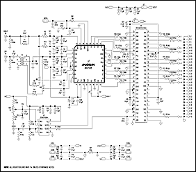
Larger Image (PDF, 210k)
Figure 1a. MAX1448 EV kit circuit schematic.
Larger Image (PDF, 175k)
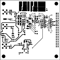
Figure 1b. MAX1448 EV kit, optimized PCB layout (component side).
Larger Image (PDF, 158k)
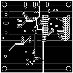
Figure 1c. MAX1448 EV kit, optimized PCB layout (solder side).
A proper test setup and the right test equipment1 are necessary to realize the performance specified for a given converter (Figure 2a and 2b).
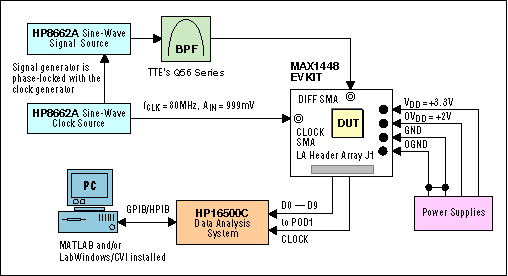
Figure 2a. System configuration to test SNR, SINAD, THD, and SFDR.
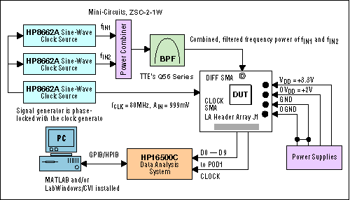
Figure 2b. System configuration to test two-tone IMD.
The following hardware² has proven to be extremely efficient and is therefore recommended for the test setup:
DC power supply: Hewlett Packard E3620A dual-supply 0-25V / 0-1A. Use separate supplies for the analog and the digital nodes. Each must provide 100mA of output drive current.
Clock-signal function generator: Hewlett-Packard HP8662A. The clock input for the device under test (DUT) accepts CMOS-compatible clock signals. This signal should have low jitter and fast rise and fall times, because the high-speed ADC has a 10-stage pipeline, and its interstage conversion depends on the repeatability of the rising and falling edges of the external clock. Sampling occurs on the falling edge of the clock signal, so edge should have the lowest possible jitter. Significant aperture jitter limits the ADC's SNR performance as follows:
 , where fIN represents the analog input frequency and tAJ is the time of the aperture jitter. Clock jitter is especially critical for undersampling applications.
Input-signal function generator: Hewlett-Packard HP8662A. For proper operation, this function generator should be phase-locked to the clock-signal generator.
Logic analyzer (LA): Hewlett-Packard HP16500C. Depending on the number of points in the proposed FFT, you may be able to capture the data using an LA with less memory depth (such as the 4k data record available in the HP1663C).
Analog bandpass filter: TTE Elliptical Function Bandpass Filter, Q56 series. Cutoff frequencies are 7.5MHz, 20MHz, 40MHz, and 50MHz.
Digital multimeters (DMMs): Various Fluke, Keithley Instruments, and HP multimeters (including the hand-held HP2373A and the AC-powered HP34401A) were used in the setup to check for proper reference, supply, and common-mode voltages.
Evaluating the DUTTo simplify evaluation of the DUT, it was tested with a performance-optimized, fully assembled and tested, surface-mount board. Follow the steps below to configure the setup and to operate this board. You should complete all the connections before turning on the power supplies or enabling the function generators.
Apply a + 3.0V analog power supply to VAIN1 and VAIN2, and connect its ground terminal to AGND. Apply a + 3.0V digital power supply to VDIN1 and VDIN2, and connect its ground terminal to DGND. Verify that no shunts are installed for jumpers JU1 (shutdown disabled) and JU2 (digital outputs enabled). Connect the clock function generator to the CLOCK SMA connector. Connect the output of the analog-signal function generator to the input of one of the bandpass filters. To evaluate differential analog signals, verify that shunts are installed on pins 1 and 2 of jumpers JU3 and JU4. Connect the output of the bandpass filter to the DIFF IN SMA connector. To evaluate single-ended analog signals, verify that shunts are installed on pins 2 and 3 of jumpers JU3 and JU4, and connect the output of the bandpass filter to the SINGLE IN SMA connector. Connect one of the logic-analyzer interface cables (pods) to the square pin header J1. Turn on both power supplies, and verify + 1.20V across test points TP 4 and TP5 with a voltmeter. If necessary, adjust potentiometer R34 to obtain + 1.20V. Enable the function generators. Set the clock function generator to its maximum output amplitude (999mV for the suggested HP8662A) and a clock frequency of fCLK = 80MHz. Set the analog signal function generator to the desired input tone, with any amplitude between 10µV and 999mV. Note that input amplitude and frequency must be selected according to the bandpass filter's corner frequency. Bandpass filters used in evaluating high-speed data converters usually have a very narrow passband. To achieve optimum performance (depending on filter type and manufacturer, of course), you should set the input tone to within 5% of the corner frequency. Because the filter attenuates the generator's output signal, set the generator's amplitude slightly higher to achieve the desired full-scale input specification. For proper operation, phase-lock the two (three, if testing for two-tone IMD) function generators. Synchro nize the LA with the external clock signal from the board, and set the LA to latch data on the clock's rising edge. Enable the LA and begin collecting data. Data can be stored on a floppy disk, on the LA's hard disk, or on a data-acquisition (DAQ) board communicating through the LA's HPIB bus. Now that the necessary steps for test setup and hardware configuration have been completed and the system is ready to capture data from the DUT, it is time to select the software tools for data capture and analysis:
LabWindows / CVI â„¢ serves as the required data capture and communications link between the LA and the DAQ controller board. (The C-based program routine used for this purpose will not be discussed in this article.) MATLAB â„¢ is a powerful tool that performs the FFT and dynamic analysis of the captured data. To help you understand how a MATLAB program routine analyzes and graphs the dynamic performance of a high-speed data converter, some of the FFT and power-spectrum basics are reviewed in the next section.
Power Spectrum, Bins, Spectral Leakage, and WindowingThe Fast Fourier Transform (FFT) and the power spectrum are powerful tools for measuring and analyzing signals from captured data records. They can capture time-domain signals, measure their frequency content, convert the results to convenient units, and display them. To perform FFT-based measurements, however, one must understand the issues and the calculations involved. Basic functions of an FFT-based signal analysis are the FFT itself and the power spectrum. Both are extremely useful for measuring the frequency content of stationary or transient signals. FFTs usually produce the average of a signal's frequency content over the time interval that the signal was acquired. Thus, FFTs are always recommended for stationary-signal analysis.
Two-Sided to Single-Sided Power-Spectrum ConversionAmong the most basic and important computations in signal analysis are the use of the FFT in converting from a two-sided to a single-sided power spectrum, adjusting the frequency resolution, and displaying the spectrum . A power spectrum usually returns a matrix containing the two-sided representation of the time-domain signal power in the frequency domain. The values ​​in this matrix are proportional to the amplitude squared of each frequency component making up the time-domain signal.
A plot of the two-sided power spectrum usually contains both negative and positive frequency components. Actual frequency-analysis tools, however, focus on the positive half of the frequency spectrum only, noting that the spectrum of a real signal is symmetrical around DC. Negative frequency information is therefore irrelevant. In a two-sided spectrum, half the energy resides in the positive frequencies and half in the negative frequencies. Therefore, to convert from a two-sided spectrum to a single-sided spectrum, you discard the second half of the matrix and multiply every point (except DC) by two.
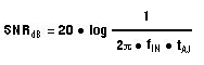
Bins and Frequency ResolutionThe frequency range and the resolution on the x-axis of a spectrum plot (see the program-code extraction below) depend on the sampling rate and the size of the data record (the number of acquisition points). The number of frequency points or lines in the power spectrum is N / 2, where N is the number of signal points captured in the time domain. The first frequency line in the power spectrum always represents DC. The last frequency line can be found at fSAMPLE / 2 -fSAMPLE / N. Frequency lines are spaced at even intervals of fSAMPLE / N, commonly referred to as a frequency bin or a FFT bin (Figure 3).
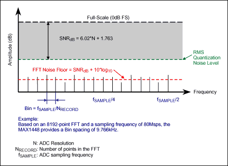
Figure 3. The representation of frequency / FFT bins in an FFT graph.
Bins can also be computed with reference to the ADC's sampling period: Bin = fSAMPLE / N = 1 / (N × Δ tSAMPLE) For example, with a sampling frequency of fSAMPLE = 82.345MHz and a record length of 8,192 data points, the distance between each frequency line in the FFT plot is exactly 10.052kHz. (Refer to Figure 1 of Defining and Testing Dynamic Parameters in High-Speed ​​ADCs, Part 1.)
The calculations for the frequency axis (x-axis) are proof that the sampling frequency determines the range or the bandwidth of the frequency spectrum. For a given sampling frequency, the number of points acquired in the time domain determines the resolution frequency. To increase the resolution for a given frequency range, the depth of the data record can be increased at the same sampling frequency (see the following program-code extraction).
% Find the signal bin number, DC = bin 1
fin = find (Dout_dB (1: numpt / 2) == maxdB);
% Span of the input frequency on each side
span = max (round (numpt / 200), 5);
% Approximate search span for harmonics on each side
spanh = 2;
% Determine power spectrum
spectP = (abs (Dout_spect)). × (abs (Dout_spect));
% Find DC offset power
Pdc = sum (spectP (1: span));
% Extract overall signal power
Ps = sum (spectP (fin-span: fin + span));
% Vector / matrix to store both frequency and power of signal and harmonics
Fh = [];
% The 1st element in the vector / matrix represents the signal, the next element represents% the 2nd harmonic, etc.
Ph = []; Spectral Leakage and Window FunctionsWindow functions are common in FFT analysis, and their proper use is critical in FFT-based measurements. The following discussion of spectral leakage stresses the need to select an appropriate window function and scale it properly for a given application. To accurately determine spectral leakage, however, it may not be enough to use adequate signal-acquisition techniques, convert a two-sided power spectrum into a single-sided one, and rescale the result. To gain a better understanding of this term, one should perform an N-point FFT on a spectrally pure sinusoidal input.
Spectral leakage is the result of an assumption in the FFT algorithm that the time record is precisely repeated throughout all time and that all signals contained in this time record are periodic at intervals corresponding to the length of the time record. However, a nonintegral number of cycles in the time record (fIN / fSAMPLE![]() NWINDOW / NRECORD) violates this condition and causes spectral leakage (Figure 4). (Refer to Appendix 2 of Part 1.) Only two cases can guarantee the acquisition of an integral number of cycles:
NWINDOW / NRECORD) violates this condition and causes spectral leakage (Figure 4). (Refer to Appendix 2 of Part 1.) Only two cases can guarantee the acquisition of an integral number of cycles:
Synchronous sampling with respect to the input tone The capture of a transient signal that fits entirely into the time record In most cases, however, the application deals with an unknown stationary3 input. This means there is no guarantee of sampling an integral number of cycles. Spectral leakage distorts the measurement by spreading the energy of a given frequency component over the adjacent frequency lines or bins. Selecting an appropriate window function can minimize the effects of this spectral leakage.
Figure 4. The effects of windows on spectral leakage.
To fully understand how a given window function affects the frequency spectrum, one must take a closer look at the frequency characteristics of windows. Windowing of the input data is equivalent to convolving the spectrum of the original signal with the spectrum of the window. Even for coherent sampling4, the signal is convolved with a rectangular-shaped window of uniform height. Such convolution shows a typical sine-function characteristic spectrum.
The real-frequency characteristic of a window is a continuous spectrum consisting of a main lobe and several side lobes. The main lobe is centered at each frequency component of the signal in the time domain. Side lobes approach zero at intervals on each side of the main lobe. An FFT, on the other hand, produces a discrete frequency spectrum. The continuous, periodic spectrum of a window is sampled by the FFT, just as an ADC would sample an input signal in the time domain. What appears in each frequency line of the FFT is the value of the continuous, convolved spectrum at each FFT frequency line.
If the frequency components of the original signal match a frequency line exactly, as is the case when you acquire an integral number of cycles, you see only the main lobe of the spectrum. Side lobes do not appear, because the window spectrum approaches zero at bin-frequency intervals on either side of the main lobe. If a time record does not contain an integral number of cycles, the continuous spectrum of the window is shifted from the main lobe center at a fraction of the frequency bin that corresponds to the difference between the frequency component and the FFT frequency lines. This shift causes side lobes to appear in the spectrum. Thus, the window's side-lobe characteristics directly affect the extent to which adjacent frequency components "leak into" the neighboring frequency bins.
Window CharacteristicsBefore choosing an appropriate window, it is necessary to define the parameters and the characteristics that enable users to compare windows. Such characteristics include the -3dB main-lobe width, the -6dB main-lobe width, the maximum side-lobe level, and the side-lobe rolloff rate (Table 1).
Side lobes of the window are characterized by the maximum side-lobe level (defined as the maximum side-lobe level in dB with respect to the main lobe's peak gain) and the side-lobe rolloff (defined as the asymptotic decay rate in dB / decade or dB / octave of frequency) of the side-lobe peaks.
Table 1. Characteristics of Frequently Used Window Functions
(Also refer to MATLAB program code)
Selecting the Right WindowDifferent windows suit different applications. To choose the right spectral window, one has to guess the signal frequency content. If the signal contains strong interfering frequency components distant from the frequency of interest, you should choose a window whose side lobes have a high-rolloff rate. If strong interfering signals are close to the frequency of interest, a window with low maximum levels of side lobe is more suitable.
If the frequency band of interest contains two or more signals close to each other, spectral resolution becomes important. In that case, a window with a narrow main lobe is better. For a single frequency component in which the focus is on amplitude accuracy rather than its precise location in the frequency bin, a window with a broad main lobe is recommended. Finally, coherent sampling (instead of a window) is recommended for a flat or broadband frequency spectrum (see the following program-code extraction).
% If no window function is used, the input tone must be chosen to be unique and with% regard to the sampling frequency. To achieve this prime numbers are introduced and the% input tone is determined by fIN = fSAMPLE × (Prime Number / Data Record Size).
% To relax this requirement, window functions such as HANNING and HAMING (see below) can% be introduced, however the fundamental in the resulting FFT spectrum appears 'sharper'% without the use of window functions.
Doutw = Dout;
% Doutw = Dout. × hanning (numpt);
% Doutw = Dout. × hamming (numpt);
% Performing the Fast Fourier Transform
Dout_spect = fft (Doutw);
% Recalculate to dB
Dout_dB = 20 × log10 (abs (Dout_spect));
% Display the results in the frequency domain with an FFT plot
figure;
maxdB = max (Dout_dB (1: numpt / 2));
The Hanning window function, which provides good frequency resolution and reduced spectral leakage, yields satisfactory results in most applications. The Flat Top window has good amplitude accuracy, but its wide main lobe provides poor frequency resolution and more spectral leakage. The Flat Top window has a lower maximum side-lobe level than does the Hanning window, but the Hanning window has a faster rolloff rate.
An application consisting of only transient signals should have no spectral windows at all, because they tend to attenuate important information at the beginning of the sample block. In the case of a transient signal, you should choose a nonspectral window such as the Force or Exponential window.
Selecting an appropriate window is not easy, but if the signal content is unknown one can start with the Hanning characteristic. It is also an excellent idea to compare the performance of multiple window functions to find the one most suitable for a given application.
Table 2. Signal Content vs. Window Selection and Advantages
Dynamic-Range Specifications SNR, SINAD, THD, and SFDRWith the knowledge you've gained from the preceding sections of this article, the following program-code extraction should be easy to understand. Based on the FFT, the power spectrum, and attention to spectral leakage and window functions, the specifications SNR, SINAD, THD, and SFDR are calculated as follows, using MATLAB: SNR = 10 × log10 (Ps / Pn)
SINAD = 10 × log10 (Ps / (Pn + Pd))
THD = 10 × log10 (Pd / Ph (1))
SFDR = 10 × log10 (Ph (1) / max (Ph (2:10))),
where Ps is signal power, Pn is noise power, Pd is distortion power caused by 2nd through 5th-order harmonics, Ph (1) is fundamental harmonic power, and Ph (2:10) is harmonic power of 2nd through 9th-order harmonics (see the following program-code extraction for the power-spectrum level).% Find harmonic frequencies and power components in the FFT spectrum
for har_num = 1: 10
% Input tones greater than fSAMPLE are aliased back into the spectrum
tone = rem ((har_num × (fin-1) +1) / numpt, 1);
if tone> 0.5
% Input tones greater than 0.5 × fSAMPLE (after aliasing) are reflected
tone = 1-tone;
end
Fh = [Fh tone];
% For this procedure to work, ensure the folded back high order harmonics do not overlap
% with DC or signal or lower order harmonics
har_peak = max (spectP (round (tone × numpt) -spanh: round (tone × numpt) + spanh));
har_bin = find (spectP (round (tone × numpt) -spanh: round (tone × numpt) + spanh) == har_peak);
har_bin = har_bin + round (tone × numpt) -spanh-1;
Ph = [Ph sum (spectP (har_bin-1: har_bin + 1))];
end
% Determine the total distortion power
Pd = sum (Ph (2: 5));
% Determine the noise power
Pn = sum (spectP (1: numpt / 2))-Pdc-Ps-Pd;
format;
A = (max (code) -min (code)) / 2 ^ numbit
AdB = 20 × log10 (A)
SINAD = 10 × log10 (Ps / (Pn + Pd))
SNR = 10 × log10 (Ps / Pn)
disp ('THD is calculated from 2nd through 5th order harmonics');
THD = 10 × log10 (Pd / Ph (1))
SFDR = 10 × log10 (Ph (1) / max (Ph (2:10)))
disp ('Signal & Harmonic Power Components:');
HD = 10 × log10 (Ph (1:10) / Ph (1))
Based on the MATLAB source code (see below), the MAX1448 was tested not only for its data sheet specifications but for many other over- and undersampling input frequencies as well. It achieved excellent dynamic performance under all conditions.% Example program routine to generate FFT plots and determine the dynamic performance of
% a high-speed dataconverter from the data records taken with a HP16500C Logic Analyzer
% System. Data was extracted through the HPIB interface and read into the following MATLAB
% program routine. The same data can be extracted from the controller interface of the LA
% and simply be copied to a floppy disk—a rather time-consuming way, but possible.
% Start MAX1448 Dynamic Performance Test Routine
filename = input ('Type a: \ filename or Press RETURN for HPIB Data Transfer:');
if isempty (filename)
filename = 'listing';
end
fid = fopen (filename, 'r');
numpt = input ('Data Record Size (Number of Points)?');
fclk = input ('Sampling Frequency (MHz)?');
% MAX1448-10-bit data converter
numbit = 10;
% Discard first 13 lines from the data file, which do not contain data
for i = 1: 13,
fgetl (fid);
end
[v1, count] = fscanf (fid, '% f', [2, numpt]);
fclose (fid);
v1 = v1 ';
code = v1 (:, 2);
% Display a warning, when the input generates a code greater than full-scale
if (max (code) == 2 ^ numbit-1) | (min (code) == 0)
disp ('Warning: ADC may be clipping !!!');
end
% Plot results in the time domain
figure;
plot ([1: numpt], code);
title ('TIME DOMAIN')
xlabel ('SAMPLES');
ylabel ('DIGITAL OUTPUT CODE');
% Recenter the digital sine wave
Dout = code- (2 ^ numbit-1) / 2;
% If no window function is used, the input tone must be chosen to be unique and with
% regard to the sampling frequency. To achieve this prime numbers are introduced and the
% input tone is determined by fIN = fSAMPLE * (Prime Number / Data Record Size).
% To relax this requirement, window functions such as HANNING and HAMING (see below) can
% be introduced, however the fundamental in the resulting FFT spectrum appears 'sharper'
% without the use of window functions.
Doutw = Dout;
% Doutw = Dout. * Hanning (numpt);
% Doutw = Dout. * Hamming (numpt);
% Performing the Fast Fourier Transform
Dout_spect = fft (Doutw);
% Recalculate to dB
Dout_dB = 20 * log10 (abs (Dout_spect));
% Display the results in the frequency domain with an FFT plot
figure;
maxdB = max (Dout_dB (1: numpt / 2));
% For TTIMD, use the following short routine, normalized to —6.5dB full-scale.
% plot ([0: numpt / 2-1]. * fclk / numpt, Dout_dB (1: numpt / 2) -maxdB-6.5);
plot ([0: numpt / 2-1]. * fclk / numpt, Dout_dB (1: numpt / 2) -maxdB);
grid on;
title ('FFT PLOT');
xlabel ('ANALOG INPUT FREQUENCY (MHz)');
ylabel ('AMPLITUDE (dB)');
a1 = axis; axis ([a1 (1) a1 (2) -120 a1 (4)]);
% Calculate SNR, SINAD, THD and SFDR values
% Find the signal bin number, DC = bin 1
fin = find (Dout_dB (1: numpt / 2) == maxdB);
% Span of the input frequency on each side
span = max (round (numpt / 200), 5);
% Approximate search span for harmonics on each side
spanh = 2;
% Determine power spectrum
spectP = (abs (Dout_spect)). * (abs (Dout_spect));
% Find DC offset power
Pdc = sum (spectP (1: span));
% Extract overall signal power
Ps = sum (spectP (fin-span: fin + span));
% Vector / matrix to store both frequency and power of signal and harmonics
Fh = [];
% The 1st element in the vector / matrix represents the signal, the next element represents
% the 2nd harmonic, etc.
Ph = [];
% Find harmonic frequencies and power components in the FFT spectrum
for har_num = 1: 10
% Input tones greater than fSAMPLE are aliased back into the spectrum
tone = rem ((har_num * (fin-1) +1) / numpt, 1);
if tone> 0.5
% Input tones greater than 0.5 * fSAMPLE (after aliasing) are reflected
tone = 1-tone;
end
Fh = [Fh tone];
% For this procedure to work, ensure the folded back high order harmonics do not overlap
% with DC or signal or lower order harmonics
har_peak = max (spectP (round (tone * numpt) -spanh: round (tone * numpt) + spanh));
har_bin = find (spectP (round (tone * numpt) -spanh: round (tone * numpt) + spanh) == har_peak);
har_bin = har_bin + round (tone * numpt) -spanh-1;
Ph = [Ph sum (spectP (har_bin-1: har_bin + 1))];
end
% Determine the total distortion power
Pd = sum (Ph (2: 5));
% Determine the noise power
Pn = sum (spectP (1: numpt / 2))-Pdc-Ps-Pd;
format;
A = (max (code) -min (code)) / 2 ^ numbit
AdB = 20 * log10 (A)
SINAD = 10 * log10 (Ps / (Pn + Pd))
SNR = 10 * log10 (Ps / Pn)
disp ('THD is calculated from 2nd through 5th order harmonics');
THD = 10 * log10 (Pd / Ph (1))
SFDR = 10 * log10 (Ph (1) / max (Ph (2:10)))
disp ('Signal & Harmonic Power Components:');
HD = 10 * log10 (Ph (1:10) / Ph (1))
% Distinguish all harmonics locations within the FFT plot
hold on;
plot (Fh (2) * fclk, 0, 'mo', Fh (3) * fclk, 0, 'cx', Fh (4) * fclk, 0, 'r +', Fh (5) * fclk, 0, 'g *', ... Fh (6) * fclk, 0, 'bs', Fh (7) * fclk, 0, 'bd', Fh (8) * fclk, 0, 'kv', Fh (9 ) * fclk, 0, 'y ^');
legend ('1st', '2nd', '3rd', '4th', '5th', '6th', '7th', '8th', '9th');
hold off; Dynamic-Range Specifications, TTIMDTwo-tone IMD can be a tricky measurement, because the additional equipment required (a power combiner to combine two input frequencies) can contribute unwanted intermodulation products that falsify the ADC's intermodulation distortion. You must observe the following conditions to optimize IMD performance, although they make the selection of proper input frequencies a tedious task. First, the input tones must fall into the passband of the input filter. If these tones are close together (several tens or hundreds of kilohertz for a megahertz bandwidth), an appropriate window function must be chosen as well. Placing them too close together, however, may allow the power combiner to falsify the overall IMD readings by contributing unwanted 2nd- and 3rd-order IMD products (depending on the input tones' location within the passband). Spacing the input tones too far apart may call for a different window type that has less frequency resolution. The se tup also requires a minimum of three phase-locked signal generators. This requirement seldom poses a problem for test labs, but generators have different capabilities for matching frequency and amplitude. Compensating such mismatches to achieve (for example) a -0.5dB FS two- tone envelope and signal amplitudes of -6.5dB FS will increase your effort and test time (see the following program-code extraction). %For TTIMD, use the following short routine, normalized to -6.5dB full-scale.
%plot([0:numpt/2-1].×fclk/numpt,Dout_dB(1:numpt/2)-maxdB-6.5);
plot([0:numpt/2-1].×fclk/numpt,Dout_dB(1:numpt/2)-maxdB);
grid on;
title('FFT PLOT');
xlabel('ANALOG INPUT FREQUENCY (MHz)');
ylabel('AMPLITUDE (dB)');
a1=axis; axis([a1(1) a1(2) -120 a1(4)]); ConclusionBesides the points above, many other issues confront an engineer trying to determine the dynamic range of a high-speed ADC by capturing its signals and analyzing them. Unfortunately, mistakes are easily made in spectral-measurement procedures. But this task of data acquisition and analysis is greatly eased by an understanding of FFT-based measurement and related computations, the effect of spectral leakage and how to prevent it, and the necessary layout techniques and equipment.
_______________________
1The MAX1444/MAX1446/MAX1448 EV kit was selected to properly evaluate dynamic performance for the 10-bit, 80Msps MAX1448.
²For any of the equipment suggested, you can substitute an item more suitable for your specific application.
3A stationary signal is present before, during, and after the data capture.
4Performing an FFT with no apparent window function selected is frequently referred to as performing the FFT with a "uniform" or "rectangular" window. Literature Sources1. MAX1448 data sheet, Rev. 0, 10/00, Maxim Integrated Products.
2. MAX1448 EV kit data sheet, Rev. 0, 0/00, Maxim Integrated Products.
3. Analog Integrated Circuit Design, D. Johns & K. Martin, John Wiley & Sons Inc., 1997.
4. Low-Voltage/Low-Power Integrated Circuits and Systems--Low-Voltage Mixed-Signal Circuits, E. Sanchez-Sinencio & AG Andreou, IEEE Press Marketing, 1999.
5. Integrated Analog-to-Digital and Digital-to-Analog Converters, R. van de Plasche, Kluwer Academic Publishers, 1994.
6. Analog-Digital Conversion Handbook, Engineering Staff of Analog Devices Inc., PTR Prentice Hall Publishers, 1986.
7. Mixed-Signal and DSP Design Techniques, Engineering Staff of Analog Devices Inc., Printed by Analog Devices, 2000.
A similar version of this article appeared in the December 2000 issue of Microwaves and RF.
Additional Information: Defining and Testing Dynamic Parameters in High-Speed ​​ADCs, Part 1
The following is a discussion of the setups and procedures recommended for testing high-speed data converters. It includes the software tools, the hardware configurations, and the instruments for data capture and analysis needed to test a new family of 10-bit, + 3V , high-speed data converters from Maxim. It also warns of traps you can encounter if equipment selection, setup configuration, layout, and FFT-based analysis are not performed with care. The following topics are covered:
Dynamic specifications and definitions Board layout and hardware configuration Power spectrum, bins, spectral leakage, and window functions Software tools for testing SNR, SINAD, THD, SFDR, and TTIMD Many approaches are available for acquiring output data from A / D converters (not just the high-speed ones) and for analyzing their dynamic performance. The methods presented here represent one proven approach, and readers are encouraged to modify them as necessary for the application at hand.
Dynamic Specifications For those who missed Part 1 of this discussion, the following is a brief overview of the definitions and the mathematical descriptions of important dynamic parameters for high-speed ADCs.
| Dynamic Parameter | Description / Definition |
| Signal-to-Noise Ratio (SNR) | SNRdB = 6.02 × N + 1.76. |
| Signal-to-Noise and Distortion Ratio (SINAD) | SINADdB = 20 × log10 (ASIGNAL [rms] / ANOISE [rms]). |
| Effective Number of Bits (ENOB) | ENOB = (SINAD-1.76) / 6.02. |
| Total Harmonic Distortion (THD) | |
| Spurious-Free Dynamic Range (SFDR) | SFDR is the ratio expressed in decibels of the rms amplitude of the fundamental (maximum signal component) to the rms value of the next-largest spurious component, excluding DC offset. |
| Two-Tone Intermodulation Distortion (TTIMD) | TTIMDdB = 20 × log10 {Σ (AIMF_SUM [rms] + AIMF_DIFF [rms]) / AFUNDAMENTAL [rms]}. IMF_SUM and IMF_DIFF in a TTIMD setup contain two input tones only. |
| Multi-Tone Intermodulation Distortion (MTIMD) | MTIMDdB = 20 × log10 {Σ (AIMF_SUM [rms] + AIMF_DIFF [rms]) / AFUNDAMENTAL [rms]}. IMF_SUM and IMF_DIFF in an MTIMD setup contains more than two (usually up to four) input tones. |
| Voltage Standing-Wave Ratio (VSWR) | VSWR = (1 + | Ï |) / (1-| Ï |), where Ï represents the reflection coefficient. |
Locate all bypass capacitors as close to the device as possible, preferably on the same side as the ADC, using surface-mount components to achieve minimum trace length, inductance, and capacitance. Bypass analog and digital supplies, references, and common-mode inputs with two 0.1µF ceramic capacitors in parallel and a 2.2µF bipolar capacitor to ground. Multilayer boards with separate ground and power planes produce the highest level of signal integrity. Consider the use of a split ground plane arranged to match the physical location of analog and digital grounds on the ADC's package. The impedance of the two ground planes must be kept as low as possible, and, to avoid possible damage or latchup, their AC and DC voltage differences (or both) must be less than 0.3V. These grounds should be joined at a single point, so that noisy digital ground currents do not interfere with the analog ground plane. The ideal location of this connection can be determined experimentally, as the point al ong the gap between the two ground planes that produces optimum results. This connection can be achieved with a low-value surface-mount resistor of 1ν to 5ν, a ferrite bead, or a direct short. As an alternative (if the ground plane is sufficiently isolated from noisy digital systems such as the downstream output buffer and DSP), all ground pins can share the same ground plane. Route high-speed digital signal traces away from sensitive analog traces. Keep all signal lines short and free of 90 ° turns . Always consider the clock input as an analog input. Route it away from actual analog inputs and other digital signal lines.
Larger Image (PDF, 210k)
Figure 1a. MAX1448 EV kit circuit schematic.
Larger Image (PDF, 175k)
Figure 1b. MAX1448 EV kit, optimized PCB layout (component side).
Larger Image (PDF, 158k)
Figure 1c. MAX1448 EV kit, optimized PCB layout (solder side).
A proper test setup and the right test equipment1 are necessary to realize the performance specified for a given converter (Figure 2a and 2b).
Figure 2a. System configuration to test SNR, SINAD, THD, and SFDR.
Figure 2b. System configuration to test two-tone IMD.
The following hardware² has proven to be extremely efficient and is therefore recommended for the test setup:
DC power supply: Hewlett Packard E3620A dual-supply 0-25V / 0-1A. Use separate supplies for the analog and the digital nodes. Each must provide 100mA of output drive current.
Clock-signal function generator: Hewlett-Packard HP8662A. The clock input for the device under test (DUT) accepts CMOS-compatible clock signals. This signal should have low jitter and fast rise and fall times, because the high-speed ADC has a 10-stage pipeline, and its interstage conversion depends on the repeatability of the rising and falling edges of the external clock. Sampling occurs on the falling edge of the clock signal, so edge should have the lowest possible jitter. Significant aperture jitter limits the ADC's SNR performance as follows:
, where fIN represents the analog input frequency and tAJ is the time of the aperture jitter. Clock jitter is especially critical for undersampling applications. Input-signal function generator: Hewlett-Packard HP8662A. For proper operation, this function generator should be phase-locked to the clock-signal generator.
Logic analyzer (LA): Hewlett-Packard HP16500C. Depending on the number of points in the proposed FFT, you may be able to capture the data using an LA with less memory depth (such as the 4k data record available in the HP1663C).
Analog bandpass filter: TTE Elliptical Function Bandpass Filter, Q56 series. Cutoff frequencies are 7.5MHz, 20MHz, 40MHz, and 50MHz.
Digital multimeters (DMMs): Various Fluke, Keithley Instruments, and HP multimeters (including the hand-held HP2373A and the AC-powered HP34401A) were used in the setup to check for proper reference, supply, and common-mode voltages.
Evaluating the DUTTo simplify evaluation of the DUT, it was tested with a performance-optimized, fully assembled and tested, surface-mount board. Follow the steps below to configure the setup and to operate this board. You should complete all the connections before turning on the power supplies or enabling the function generators.
Apply a + 3.0V analog power supply to VAIN1 and VAIN2, and connect its ground terminal to AGND. Apply a + 3.0V digital power supply to VDIN1 and VDIN2, and connect its ground terminal to DGND. Verify that no shunts are installed for jumpers JU1 (shutdown disabled) and JU2 (digital outputs enabled). Connect the clock function generator to the CLOCK SMA connector. Connect the output of the analog-signal function generator to the input of one of the bandpass filters. To evaluate differential analog signals, verify that shunts are installed on pins 1 and 2 of jumpers JU3 and JU4. Connect the output of the bandpass filter to the DIFF IN SMA connector. To evaluate single-ended analog signals, verify that shunts are installed on pins 2 and 3 of jumpers JU3 and JU4, and connect the output of the bandpass filter to the SINGLE IN SMA connector. Connect one of the logic-analyzer interface cables (pods) to the square pin header J1. Turn on both power supplies, and verify + 1.20V across test points TP 4 and TP5 with a voltmeter. If necessary, adjust potentiometer R34 to obtain + 1.20V. Enable the function generators. Set the clock function generator to its maximum output amplitude (999mV for the suggested HP8662A) and a clock frequency of fCLK = 80MHz. Set the analog signal function generator to the desired input tone, with any amplitude between 10µV and 999mV. Note that input amplitude and frequency must be selected according to the bandpass filter's corner frequency. Bandpass filters used in evaluating high-speed data converters usually have a very narrow passband. To achieve optimum performance (depending on filter type and manufacturer, of course), you should set the input tone to within 5% of the corner frequency. Because the filter attenuates the generator's output signal, set the generator's amplitude slightly higher to achieve the desired full-scale input specification. For proper operation, phase-lock the two (three, if testing for two-tone IMD) function generators. Synchro nize the LA with the external clock signal from the board, and set the LA to latch data on the clock's rising edge. Enable the LA and begin collecting data. Data can be stored on a floppy disk, on the LA's hard disk, or on a data-acquisition (DAQ) board communicating through the LA's HPIB bus. Now that the necessary steps for test setup and hardware configuration have been completed and the system is ready to capture data from the DUT, it is time to select the software tools for data capture and analysis:
LabWindows / CVI â„¢ serves as the required data capture and communications link between the LA and the DAQ controller board. (The C-based program routine used for this purpose will not be discussed in this article.) MATLAB â„¢ is a powerful tool that performs the FFT and dynamic analysis of the captured data. To help you understand how a MATLAB program routine analyzes and graphs the dynamic performance of a high-speed data converter, some of the FFT and power-spectrum basics are reviewed in the next section.
Power Spectrum, Bins, Spectral Leakage, and WindowingThe Fast Fourier Transform (FFT) and the power spectrum are powerful tools for measuring and analyzing signals from captured data records. They can capture time-domain signals, measure their frequency content, convert the results to convenient units, and display them. To perform FFT-based measurements, however, one must understand the issues and the calculations involved. Basic functions of an FFT-based signal analysis are the FFT itself and the power spectrum. Both are extremely useful for measuring the frequency content of stationary or transient signals. FFTs usually produce the average of a signal's frequency content over the time interval that the signal was acquired. Thus, FFTs are always recommended for stationary-signal analysis.
Two-Sided to Single-Sided Power-Spectrum ConversionAmong the most basic and important computations in signal analysis are the use of the FFT in converting from a two-sided to a single-sided power spectrum, adjusting the frequency resolution, and displaying the spectrum . A power spectrum usually returns a matrix containing the two-sided representation of the time-domain signal power in the frequency domain. The values ​​in this matrix are proportional to the amplitude squared of each frequency component making up the time-domain signal.
A plot of the two-sided power spectrum usually contains both negative and positive frequency components. Actual frequency-analysis tools, however, focus on the positive half of the frequency spectrum only, noting that the spectrum of a real signal is symmetrical around DC. Negative frequency information is therefore irrelevant. In a two-sided spectrum, half the energy resides in the positive frequencies and half in the negative frequencies. Therefore, to convert from a two-sided spectrum to a single-sided spectrum, you discard the second half of the matrix and multiply every point (except DC) by two.
Bins and Frequency ResolutionThe frequency range and the resolution on the x-axis of a spectrum plot (see the program-code extraction below) depend on the sampling rate and the size of the data record (the number of acquisition points). The number of frequency points or lines in the power spectrum is N / 2, where N is the number of signal points captured in the time domain. The first frequency line in the power spectrum always represents DC. The last frequency line can be found at fSAMPLE / 2 -fSAMPLE / N. Frequency lines are spaced at even intervals of fSAMPLE / N, commonly referred to as a frequency bin or a FFT bin (Figure 3).
Figure 3. The representation of frequency / FFT bins in an FFT graph.
Bins can also be computed with reference to the ADC's sampling period: Bin = fSAMPLE / N = 1 / (N × Δ tSAMPLE) For example, with a sampling frequency of fSAMPLE = 82.345MHz and a record length of 8,192 data points, the distance between each frequency line in the FFT plot is exactly 10.052kHz. (Refer to Figure 1 of Defining and Testing Dynamic Parameters in High-Speed ​​ADCs, Part 1.)
The calculations for the frequency axis (x-axis) are proof that the sampling frequency determines the range or the bandwidth of the frequency spectrum. For a given sampling frequency, the number of points acquired in the time domain determines the resolution frequency. To increase the resolution for a given frequency range, the depth of the data record can be increased at the same sampling frequency (see the following program-code extraction).
% Find the signal bin number, DC = bin 1
fin = find (Dout_dB (1: numpt / 2) == maxdB);
% Span of the input frequency on each side
span = max (round (numpt / 200), 5);
% Approximate search span for harmonics on each side
spanh = 2;
% Determine power spectrum
spectP = (abs (Dout_spect)). × (abs (Dout_spect));
% Find DC offset power
Pdc = sum (spectP (1: span));
% Extract overall signal power
Ps = sum (spectP (fin-span: fin + span));
% Vector / matrix to store both frequency and power of signal and harmonics
Fh = [];
% The 1st element in the vector / matrix represents the signal, the next element represents% the 2nd harmonic, etc.
Ph = []; Spectral Leakage and Window FunctionsWindow functions are common in FFT analysis, and their proper use is critical in FFT-based measurements. The following discussion of spectral leakage stresses the need to select an appropriate window function and scale it properly for a given application. To accurately determine spectral leakage, however, it may not be enough to use adequate signal-acquisition techniques, convert a two-sided power spectrum into a single-sided one, and rescale the result. To gain a better understanding of this term, one should perform an N-point FFT on a spectrally pure sinusoidal input.
Spectral leakage is the result of an assumption in the FFT algorithm that the time record is precisely repeated throughout all time and that all signals contained in this time record are periodic at intervals corresponding to the length of the time record. However, a nonintegral number of cycles in the time record (fIN / fSAMPLE
Synchronous sampling with respect to the input tone The capture of a transient signal that fits entirely into the time record In most cases, however, the application deals with an unknown stationary3 input. This means there is no guarantee of sampling an integral number of cycles. Spectral leakage distorts the measurement by spreading the energy of a given frequency component over the adjacent frequency lines or bins. Selecting an appropriate window function can minimize the effects of this spectral leakage.
Figure 4. The effects of windows on spectral leakage.
To fully understand how a given window function affects the frequency spectrum, one must take a closer look at the frequency characteristics of windows. Windowing of the input data is equivalent to convolving the spectrum of the original signal with the spectrum of the window. Even for coherent sampling4, the signal is convolved with a rectangular-shaped window of uniform height. Such convolution shows a typical sine-function characteristic spectrum.
The real-frequency characteristic of a window is a continuous spectrum consisting of a main lobe and several side lobes. The main lobe is centered at each frequency component of the signal in the time domain. Side lobes approach zero at intervals on each side of the main lobe. An FFT, on the other hand, produces a discrete frequency spectrum. The continuous, periodic spectrum of a window is sampled by the FFT, just as an ADC would sample an input signal in the time domain. What appears in each frequency line of the FFT is the value of the continuous, convolved spectrum at each FFT frequency line.
If the frequency components of the original signal match a frequency line exactly, as is the case when you acquire an integral number of cycles, you see only the main lobe of the spectrum. Side lobes do not appear, because the window spectrum approaches zero at bin-frequency intervals on either side of the main lobe. If a time record does not contain an integral number of cycles, the continuous spectrum of the window is shifted from the main lobe center at a fraction of the frequency bin that corresponds to the difference between the frequency component and the FFT frequency lines. This shift causes side lobes to appear in the spectrum. Thus, the window's side-lobe characteristics directly affect the extent to which adjacent frequency components "leak into" the neighboring frequency bins.
Window CharacteristicsBefore choosing an appropriate window, it is necessary to define the parameters and the characteristics that enable users to compare windows. Such characteristics include the -3dB main-lobe width, the -6dB main-lobe width, the maximum side-lobe level, and the side-lobe rolloff rate (Table 1).
Side lobes of the window are characterized by the maximum side-lobe level (defined as the maximum side-lobe level in dB with respect to the main lobe's peak gain) and the side-lobe rolloff (defined as the asymptotic decay rate in dB / decade or dB / octave of frequency) of the side-lobe peaks.
Table 1. Characteristics of Frequently Used Window Functions
(Also refer to MATLAB program code)
| Window Type | -3dB Main-Lobe Width | -6dB Main-Lobe Width | Maximum Side-Lobe Level | Side-Lobe Rolloff Rate |
| No Window (Uniform) | 0.89 bins | 1.21 bins | -13dB | 20dB / decade, 6dB / octave |
| Hanning | 1.44 bins | 2.00 bins | -32dB | 60dB / decade, 18dB / octave |
| Hamming | 1.30 bins | 1.81 bins | -43dB | 20dB / decade, 6dB / octave |
| Flat Top | 2.94 bins | 3.56 bins | -44dB | 20dB / decade, 6dB / octave |
If the frequency band of interest contains two or more signals close to each other, spectral resolution becomes important. In that case, a window with a narrow main lobe is better. For a single frequency component in which the focus is on amplitude accuracy rather than its precise location in the frequency bin, a window with a broad main lobe is recommended. Finally, coherent sampling (instead of a window) is recommended for a flat or broadband frequency spectrum (see the following program-code extraction).
% If no window function is used, the input tone must be chosen to be unique and with% regard to the sampling frequency. To achieve this prime numbers are introduced and the% input tone is determined by fIN = fSAMPLE × (Prime Number / Data Record Size).
% To relax this requirement, window functions such as HANNING and HAMING (see below) can% be introduced, however the fundamental in the resulting FFT spectrum appears 'sharper'% without the use of window functions.
Doutw = Dout;
% Doutw = Dout. × hanning (numpt);
% Doutw = Dout. × hamming (numpt);
% Performing the Fast Fourier Transform
Dout_spect = fft (Doutw);
% Recalculate to dB
Dout_dB = 20 × log10 (abs (Dout_spect));
% Display the results in the frequency domain with an FFT plot
figure;
maxdB = max (Dout_dB (1: numpt / 2));
The Hanning window function, which provides good frequency resolution and reduced spectral leakage, yields satisfactory results in most applications. The Flat Top window has good amplitude accuracy, but its wide main lobe provides poor frequency resolution and more spectral leakage. The Flat Top window has a lower maximum side-lobe level than does the Hanning window, but the Hanning window has a faster rolloff rate.
An application consisting of only transient signals should have no spectral windows at all, because they tend to attenuate important information at the beginning of the sample block. In the case of a transient signal, you should choose a nonspectral window such as the Force or Exponential window.
Selecting an appropriate window is not easy, but if the signal content is unknown one can start with the Hanning characteristic. It is also an excellent idea to compare the performance of multiple window functions to find the one most suitable for a given application.
Table 2. Signal Content vs. Window Selection and Advantages
| Window Type | Signal Content | Window Characteristics |
| No Window (Uniform) | Broad-band random, closely spaced sine-wave signals | Narrow main lobe, slow rolloff rate, poor frequency resolution |
| Hanning | Narrow-band random signals, nature of content is unknown, sine-wave or combination of sine-wave signals | High maximum side-lobe level, good frequency resolution, reduced leakage, faster rolloff rate |
| Hamming | Closely spaced sine-wave signals | Good spectral resolution, narrow main lobe |
| Flat Top | Sine wave with need for amplitude accuracy | Good amplitude accuracy, wide main lobe, poor frequency resolution, more spectral leakage |
SINAD = 10 × log10 (Ps / (Pn + Pd))
THD = 10 × log10 (Pd / Ph (1))
SFDR = 10 × log10 (Ph (1) / max (Ph (2:10))),
where Ps is signal power, Pn is noise power, Pd is distortion power caused by 2nd through 5th-order harmonics, Ph (1) is fundamental harmonic power, and Ph (2:10) is harmonic power of 2nd through 9th-order harmonics (see the following program-code extraction for the power-spectrum level).% Find harmonic frequencies and power components in the FFT spectrum
for har_num = 1: 10
% Input tones greater than fSAMPLE are aliased back into the spectrum
tone = rem ((har_num × (fin-1) +1) / numpt, 1);
if tone> 0.5
% Input tones greater than 0.5 × fSAMPLE (after aliasing) are reflected
tone = 1-tone;
end
Fh = [Fh tone];
% For this procedure to work, ensure the folded back high order harmonics do not overlap
% with DC or signal or lower order harmonics
har_peak = max (spectP (round (tone × numpt) -spanh: round (tone × numpt) + spanh));
har_bin = find (spectP (round (tone × numpt) -spanh: round (tone × numpt) + spanh) == har_peak);
har_bin = har_bin + round (tone × numpt) -spanh-1;
Ph = [Ph sum (spectP (har_bin-1: har_bin + 1))];
end
% Determine the total distortion power
Pd = sum (Ph (2: 5));
% Determine the noise power
Pn = sum (spectP (1: numpt / 2))-Pdc-Ps-Pd;
format;
A = (max (code) -min (code)) / 2 ^ numbit
AdB = 20 × log10 (A)
SINAD = 10 × log10 (Ps / (Pn + Pd))
SNR = 10 × log10 (Ps / Pn)
disp ('THD is calculated from 2nd through 5th order harmonics');
THD = 10 × log10 (Pd / Ph (1))
SFDR = 10 × log10 (Ph (1) / max (Ph (2:10)))
disp ('Signal & Harmonic Power Components:');
HD = 10 × log10 (Ph (1:10) / Ph (1))
Based on the MATLAB source code (see below), the MAX1448 was tested not only for its data sheet specifications but for many other over- and undersampling input frequencies as well. It achieved excellent dynamic performance under all conditions.% Example program routine to generate FFT plots and determine the dynamic performance of
% a high-speed dataconverter from the data records taken with a HP16500C Logic Analyzer
% System. Data was extracted through the HPIB interface and read into the following MATLAB
% program routine. The same data can be extracted from the controller interface of the LA
% and simply be copied to a floppy disk—a rather time-consuming way, but possible.
% Start MAX1448 Dynamic Performance Test Routine
if isempty (filename)
filename = 'listing';
end
fid = fopen (filename, 'r');
numpt = input ('Data Record Size (Number of Points)?');
fclk = input ('Sampling Frequency (MHz)?');
% MAX1448-10-bit data converter
numbit = 10;
% Discard first 13 lines from the data file, which do not contain data
for i = 1: 13,
fgetl (fid);
end
[v1, count] = fscanf (fid, '% f', [2, numpt]);
fclose (fid);
v1 = v1 ';
code = v1 (:, 2);
% Display a warning, when the input generates a code greater than full-scale
if (max (code) == 2 ^ numbit-1) | (min (code) == 0)
disp ('Warning: ADC may be clipping !!!');
end
% Plot results in the time domain
figure;
plot ([1: numpt], code);
title ('TIME DOMAIN')
xlabel ('SAMPLES');
ylabel ('DIGITAL OUTPUT CODE');
% Recenter the digital sine wave
Dout = code- (2 ^ numbit-1) / 2;
% If no window function is used, the input tone must be chosen to be unique and with
% regard to the sampling frequency. To achieve this prime numbers are introduced and the
% input tone is determined by fIN = fSAMPLE * (Prime Number / Data Record Size).
% To relax this requirement, window functions such as HANNING and HAMING (see below) can
% be introduced, however the fundamental in the resulting FFT spectrum appears 'sharper'
% without the use of window functions.
Doutw = Dout;
% Doutw = Dout. * Hanning (numpt);
% Doutw = Dout. * Hamming (numpt);
% Performing the Fast Fourier Transform
Dout_spect = fft (Doutw);
% Recalculate to dB
Dout_dB = 20 * log10 (abs (Dout_spect));
% Display the results in the frequency domain with an FFT plot
figure;
maxdB = max (Dout_dB (1: numpt / 2));
% For TTIMD, use the following short routine, normalized to —6.5dB full-scale.
% plot ([0: numpt / 2-1]. * fclk / numpt, Dout_dB (1: numpt / 2) -maxdB-6.5);
plot ([0: numpt / 2-1]. * fclk / numpt, Dout_dB (1: numpt / 2) -maxdB);
grid on;
title ('FFT PLOT');
xlabel ('ANALOG INPUT FREQUENCY (MHz)');
ylabel ('AMPLITUDE (dB)');
a1 = axis; axis ([a1 (1) a1 (2) -120 a1 (4)]);
% Calculate SNR, SINAD, THD and SFDR values
% Find the signal bin number, DC = bin 1
fin = find (Dout_dB (1: numpt / 2) == maxdB);
% Span of the input frequency on each side
span = max (round (numpt / 200), 5);
% Approximate search span for harmonics on each side
spanh = 2;
% Determine power spectrum
spectP = (abs (Dout_spect)). * (abs (Dout_spect));
% Find DC offset power
Pdc = sum (spectP (1: span));
% Extract overall signal power
Ps = sum (spectP (fin-span: fin + span));
% Vector / matrix to store both frequency and power of signal and harmonics
Fh = [];
% The 1st element in the vector / matrix represents the signal, the next element represents
% the 2nd harmonic, etc.
Ph = [];
% Find harmonic frequencies and power components in the FFT spectrum
for har_num = 1: 10
% Input tones greater than fSAMPLE are aliased back into the spectrum
tone = rem ((har_num * (fin-1) +1) / numpt, 1);
if tone> 0.5
% Input tones greater than 0.5 * fSAMPLE (after aliasing) are reflected
tone = 1-tone;
end
Fh = [Fh tone];
% For this procedure to work, ensure the folded back high order harmonics do not overlap
% with DC or signal or lower order harmonics
har_peak = max (spectP (round (tone * numpt) -spanh: round (tone * numpt) + spanh));
har_bin = find (spectP (round (tone * numpt) -spanh: round (tone * numpt) + spanh) == har_peak);
har_bin = har_bin + round (tone * numpt) -spanh-1;
Ph = [Ph sum (spectP (har_bin-1: har_bin + 1))];
end
% Determine the total distortion power
Pd = sum (Ph (2: 5));
% Determine the noise power
Pn = sum (spectP (1: numpt / 2))-Pdc-Ps-Pd;
format;
A = (max (code) -min (code)) / 2 ^ numbit
AdB = 20 * log10 (A)
SINAD = 10 * log10 (Ps / (Pn + Pd))
SNR = 10 * log10 (Ps / Pn)
disp ('THD is calculated from 2nd through 5th order harmonics');
THD = 10 * log10 (Pd / Ph (1))
SFDR = 10 * log10 (Ph (1) / max (Ph (2:10)))
disp ('Signal & Harmonic Power Components:');
HD = 10 * log10 (Ph (1:10) / Ph (1))
% Distinguish all harmonics locations within the FFT plot
hold on;
plot (Fh (2) * fclk, 0, 'mo', Fh (3) * fclk, 0, 'cx', Fh (4) * fclk, 0, 'r +', Fh (5) * fclk, 0, 'g *', ... Fh (6) * fclk, 0, 'bs', Fh (7) * fclk, 0, 'bd', Fh (8) * fclk, 0, 'kv', Fh (9 ) * fclk, 0, 'y ^');
legend ('1st', '2nd', '3rd', '4th', '5th', '6th', '7th', '8th', '9th');
hold off; Dynamic-Range Specifications, TTIMDTwo-tone IMD can be a tricky measurement, because the additional equipment required (a power combiner to combine two input frequencies) can contribute unwanted intermodulation products that falsify the ADC's intermodulation distortion. You must observe the following conditions to optimize IMD performance, although they make the selection of proper input frequencies a tedious task. First, the input tones must fall into the passband of the input filter. If these tones are close together (several tens or hundreds of kilohertz for a megahertz bandwidth), an appropriate window function must be chosen as well. Placing them too close together, however, may allow the power combiner to falsify the overall IMD readings by contributing unwanted 2nd- and 3rd-order IMD products (depending on the input tones' location within the passband). Spacing the input tones too far apart may call for a different window type that has less frequency resolution. The se tup also requires a minimum of three phase-locked signal generators. This requirement seldom poses a problem for test labs, but generators have different capabilities for matching frequency and amplitude. Compensating such mismatches to achieve (for example) a -0.5dB FS two- tone envelope and signal amplitudes of -6.5dB FS will increase your effort and test time (see the following program-code extraction). %For TTIMD, use the following short routine, normalized to -6.5dB full-scale.
%plot([0:numpt/2-1].×fclk/numpt,Dout_dB(1:numpt/2)-maxdB-6.5);
plot([0:numpt/2-1].×fclk/numpt,Dout_dB(1:numpt/2)-maxdB);
grid on;
title('FFT PLOT');
xlabel('ANALOG INPUT FREQUENCY (MHz)');
ylabel('AMPLITUDE (dB)');
a1=axis; axis([a1(1) a1(2) -120 a1(4)]); ConclusionBesides the points above, many other issues confront an engineer trying to determine the dynamic range of a high-speed ADC by capturing its signals and analyzing them. Unfortunately, mistakes are easily made in spectral-measurement procedures. But this task of data acquisition and analysis is greatly eased by an understanding of FFT-based measurement and related computations, the effect of spectral leakage and how to prevent it, and the necessary layout techniques and equipment.
_______________________
1The MAX1444/MAX1446/MAX1448 EV kit was selected to properly evaluate dynamic performance for the 10-bit, 80Msps MAX1448.
²For any of the equipment suggested, you can substitute an item more suitable for your specific application.
3A stationary signal is present before, during, and after the data capture.
4Performing an FFT with no apparent window function selected is frequently referred to as performing the FFT with a "uniform" or "rectangular" window. Literature Sources1. MAX1448 data sheet, Rev. 0, 10/00, Maxim Integrated Products.
2. MAX1448 EV kit data sheet, Rev. 0, 0/00, Maxim Integrated Products.
3. Analog Integrated Circuit Design, D. Johns & K. Martin, John Wiley & Sons Inc., 1997.
4. Low-Voltage/Low-Power Integrated Circuits and Systems--Low-Voltage Mixed-Signal Circuits, E. Sanchez-Sinencio & AG Andreou, IEEE Press Marketing, 1999.
5. Integrated Analog-to-Digital and Digital-to-Analog Converters, R. van de Plasche, Kluwer Academic Publishers, 1994.
6. Analog-Digital Conversion Handbook, Engineering Staff of Analog Devices Inc., PTR Prentice Hall Publishers, 1986.
7. Mixed-Signal and DSP Design Techniques, Engineering Staff of Analog Devices Inc., Printed by Analog Devices, 2000.
A similar version of this article appeared in the December 2000 issue of Microwaves and RF.
Product categories of Storage Battery, we are specialized in manufacturers from China,Storage Battery Supplier suppliers/factory, wholesale high-quality products of manufacturing, we have the perfect after-sales service and technical support. Look forward to your cooperation!
Storage Battery
Solar Battery,Storage Battery,Solar Storage Battery,Solar Energe Storage Battery
Changxing Deli Technology Co., Ltd. , https://www.delipowers.com