Q: I am a bit confused about how to handle the analog ground and digital ground pins in the ADC. It is usually required to connect the analog ground and the digital ground on the device, but I don't want to connect the ADC to the star ground point of the system. what should I do?
A: First of all, you don't have to feel so bad about the implications of analog and digital. Many people are like this! Many of the confusion comes first from the name of the ADC ground pin. The pin names of analog ground and digital ground indicate the role of the internal components themselves, and do not necessarily mean that the external should also be done according to internal functions. Let us explain.
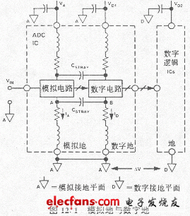
An integrated circuit has two parts, an analog circuit and a digital circuit, such as an ADC. In order to avoid the digital signal being coupled into the analog circuit, the analog ground and the digital ground are usually separated. Figure 12–1 shows a simple schematic of an ADC. The wire bond inductance and resistance resulting from the solder joints on the chip to the package leads are not specifically added by the IC designer. The rapidly changing digital current produces a voltage at point B that is necessarily coupled to point A of the analog circuit via a stray capacitance (C STRAY ). Although this is an issue that IC designers should consider when manufacturing chips. However, you can see that in order to prevent further coupling, the analog ground and digital ground pins should be connected to the same low impedance ground plane with the shortest wire on the outside. Any external impedance attached to the digital ground pin will cause a large digital noise at point B. Large digital noise is then coupled to the analog circuit through stray capacitance. This can be illustrated by a very simple schematic (Fig. 12?1).
Q: Well, you have told me to connect the analog ground and digital ground pins of the integrated circuit to the same ground plane, but I still have to separate the analog and digital ground planes in the system. I want them to be connected at only one point. Get up, but this common point is the return end of the power supply and is connected to the base ground line. So what do I have to do now?
A: If your system has only one data converter, you can actually do it as described in the product description and connect the analog ground and digital ground system to the converter. The star ground point of your system is now on the data converter. But this may be extremely undesirable, unless you start with this idea to design your system. If you have several data converters arranged on different printed circuit boards, this rule should not be used as an alternative because analog ground and digital ground systems are connected to each converter on many printed circuit boards. This is the best advice for ground loops.
Q: I can already imagine it! If I have to connect the analog ground and digital ground pins on the device, I still need to separate the analog ground and digital ground of the system. I connect the analog ground and the digital ground. Go to the analog ground plane on the printed circuit board, or the digital ground plane, but not both, right? Because the ADC is both an analog device and a digital device, which ground plane is more suitable?
A: Yes! If you connect the analog ground and digital ground pins to the digital ground plane, then your analog input signal will have digital noise superimposed because the analog input signal is single-ended and relative to the analog ground plane. .
Q: So the correct answer is to connect both the analog ground and the digital ground pins to the analog ground plane, right? But will this add digital noise to the otherwise good ground plane? Since the output signal is now relative to the analog ground plane, and all other logic is relative to the digital ground plane, will the output logic noise margin decrease? I intend to connect the ADC output to the tristate data bus on the back of the printed circuit board. There is a lot of noise there, so I think we need all the noise margins we can get first.
A: Good! No one can say that life is easy! You have got the right conclusion through the difficult road, but you propose digital noise on the analog ground plane and reduce the noise margin at the ADC output (noise The problem of margins is actually not as bad as imagined, and they can be overcome. Adding hundreds of millivolts of unreliable signals to the digital interface is significantly better than applying the same unreliable signal to the analog input. For a 16-bit ADC with a 10 V input, the least significant signal is only 150 μV! The digital ground current on the digital ground pin can't actually be worse than this, otherwise they will invalidate the analog part inside the ADC first! You bypass the high frequency noise by connecting a high quality high frequency ceramic capacitor (0 ?1μF) from the ADC supply pin to the analog ground plane. You will isolate these currents into a very small area around the integrated circuit and The impact on the rest of the system is minimized.
Although digital noise margins are reduced, if less than a few hundred millivolts, it is generally acceptable for TTL and CMOS logic. If your ADC has a single-ended ECL output, you will need to add a push-pull gate to each digital gate to balance and compensate for the output. These gate package block grounds are routed to the analog ground plane and the logic signal interface is connected differentially. Use a differential line receiver at the other end and connect its ground terminal to the digital ground plane. The noise between the analog ground plane and the digital ground plane is a common mode signal, and most of them will be attenuated at the output of the differential line receiver. You can use the same method for TTL and CMOS, but they usually have enough noise margin, so no differential transmission is needed.
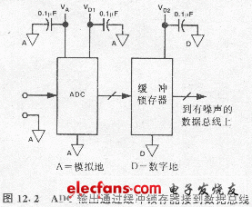
But one thing you said made me very worried. It is very frivolous to connect the ADC output directly to a noisy data bus. Bus noise can be returned to the ADC analog input via internal parasitic capacitive coupling. The parasitic capacitance is from 0?1 to 0?5 pF. It is much better if you connect the ADC output directly to the intermediate buffer latch near the ADC (see Figure 12?2). The buffer latch ground is connected to the digital ground plane, so its output logic level is compatible with the logic levels of the rest of the system.
Fiber Optic Patch Cord is important of optical network.they have same or different connectors which are installed on the end of fiber optic cable. The Fiber Optic Patch Cord series comes with a comprehensive collection of lengths and connectors to fulfill your demand for the deployment.
SC To FC Fiber Optic Patch Cord
Fiber Patch Cord,Fiber Patch Cables,Bulk Fiber Optic Cable,FC SC Fiber Patch Cord
Chengdu Xinruixin Optical Communication Technology Co.,Ltd , https://www.xrxoptics.com