0 Preface
Product testing is a concern for both manufacturers and users. In the production process, testing is an indispensable part, and some are a process in the process. Electromagnetic relays are commonly used switching components in power systems and other electrical control systems. Their reliability is an important guarantee for the reliable operation of power systems and other electrical control systems. Therefore, the characteristic parameters of relays must be accurately tested. The electrical parameters of the electromagnetic relay mainly include coil resistance, contact contact resistance, pull-in voltage, release voltage, pull-in time, and release time. These parameters are of great significance for studying the reliability and dynamic performance of relays, and are important parameters to ensure their quality characteristics.
1 system overall architecture
1.1 System Hardware Structure
The system hardware mainly includes UART serial communication module, JTAG interface module, test result display module, detection program storage module FLASH, detection circuit module and SRAM module. The overall hardware structure of the system is shown in Figure 1.
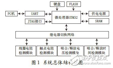
1.2 System Microprocessor
The system is mainly composed of a detection part and a display control part. In this design, the high performance ARM Cortex chip STM32F103ZET6 is used.
The chip uses a Harvard architecture inside, which integrates 64 KB of RAM and 512 KB of FLASH, and has the characteristics of fast operation, small size and low power consumption, which can fully meet the requirements of this design. The Cortex-M3 is a 32-bit core that uses Tail-Chaining interrupt technology to reduce the number of clock cycles by up to 12 clock cycles. Hardware-based interrupt processing typically reduces interrupts by 70%. The Cortex-M3 also features a new single-wire (Single Wire) technology that enables independent pin debugging.
1.3 System Workflow
After the system is powered on, first complete the initialization of each register, and then wait for the start of the detection command; click the START command on the host computer interface, then the host computer sends a start detection command to the microcontroller; the microcontroller starts to the detection circuit after receiving the start command. Send the detection command, then the MCU processes the data sent back by the detection circuit, and obtains the parameters of the relay, and displays these parameters on the interface of the host computer through the serial port.
2 system hardware design
2.1 Drive voltage design
In order to accurately measure the pull-in voltage of the relay, it is necessary to obtain a voltage source that increases from a certain amount according to a certain amount. The smaller the voltage amount is, the more accurate the test result is, but the more complicated the required circuit is. So we must find a balance between the two according to the actual requirements. Figure 2 shows the system drive voltage circuit.
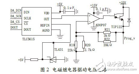
In Figure 2, the TL431 is used to provide a 2.5 V reference to the TLC5615, DA_DIN is the serial data input, DA_CS is the active-low chip select signal input, DA_SCK is the serial clock input, and DOUT is used for Cascaded serial data output, OUT is the DAC analog voltage output, which outputs an analog signal. Since the analog signal output from the TLC5615 is small and cannot drive the relay, the design is followed by an amplifying voltage circuit and an amplifying current circuit.
2.2 Design of integrated switching network
The integrated switching network of the system is completed by using the switching working principle of the relay, and the different commands issued by the single-chip microcomputer are used to control the closing of the relay, thereby switching to different test circuit modules. When testing the pull-in/release voltage, the ARM Cortex first issues an instruction to test the pull-in/release voltage. The integrated switching network switches to the Prog_v side according to the command, and the XQ1I connects one end of the measured relay contact. The specific circuit is shown in Figure 3.
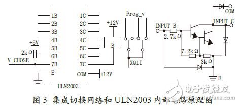
In order to solve the problem of insufficient I/O driving capability of the single chip microcomputer, ULN2003 is selected as the driving chip of the relay. ULN2003 is a high voltage and high current Darlington transistor array circuit with high operating ground voltage, high operating current, sink current up to 500 mA, and can withstand 50 V in the off state. The output can also be paralleled at high load current. run. It uses open collector output and large output current, so it can directly drive the relay. Each pair of Darlington tubes in the ULN2003 is connected in series with a 2.7 kΩ base resistor. It can be directly connected to TTL and CMOS circuits at 5 V operating voltage, allowing direct processing of data that would otherwise require standard logic buffers to process. Usually, when the microcontroller is driven by ULN2003, the 2 kΩ resistor is pulled up. At the same time, the COM pin should be left floating or connected to the power supply.
2.3 Data processing and communication with the host computer
The received data is connected to the 3.3 V conversion chip MAX232 through the asynchronous serial port. The external serial cable communicates with the PC to receive and transmit data. The STM32 acts as the lower computer to receive the instructions of the upper computer and control each part of the circuit and process the data. Then the data is sent to the host computer, the PC receives the data, and the received data is displayed through the interface through VC programming. Here, the VC of the PC sends a command to the STM32 through the serial port, and the main control chip receives the command and judges that it is valid, and then starts the control circuit to work [6]. Due to space limitations, this article does not provide a detailed description of the minimum system hardware portion of the STM32.
1- Output wave type: pure sine wave, suitable for home load, perceptual negative download.
2- Inverter box: the whole shell is made of aluminum alloy material
3- Casters: it is with casters when inverter more than 4kw, convenient for you to move the machine
4- Display, clear LCD display, easy to observe operating conditions.
5- Control: microcomputer (CPU) control technology, superior performance and stability.
6- Temperature control fan: when the box temperature reaches 35 degrees, the fan start to work automatically.
7- Protection function: built-in loading, short circuit, under-voltage, over-pressure, over-temperature protection function, high reliability.
8- Battery protection: valve-Controller maintenance-free lead-acid battery, intelligent battery management, overcharge, over-discharge protection, prolong battery life.
Off-grid Wind Solar Hybrid Inverter
Off-Grid Wind Solar Hybrid Inverter,Variable Frequency Inverter,Pure Sine Wave Power Inverter,Pure Sine Wave Solar Inverter
Delight Eco Energy Supplies Co., Ltd. , https://www.cndelight.com