With the comprehensive improvement of light output, energy efficiency and cost of high-brightness light-emitting diodes (HB-LEDs), combined with the advantages of compact, low-voltage operation and environmental protection, LED lighting (also known as solid-state lighting (SSL)) is setting off a field. Lighting revolution. In the trend of energy saving and environmental protection, LED lighting has naturally become the target of many regulatory agencies. For example, the 1.1 version of the US Department of Energy's "Energy Star" project has entered into force since February 2009. China's China National Institute of Standardization is also taking the lead in cooperating with relevant organizations to prepare for the release of the Chinese version of LED lighting energy efficiency standards in 2010.
As far as the new version of ENERGY STAR's solid-state lighting standards is concerned, an important feature of this standard is that it requires a minimum of 0.7 power factor for a variety of residential lighting products. Some of the typical products include portable desk lamps, cabinet lights and outdoor corridors. Lights, etc. This type of LED lighting application typically has a power range of 1 to 12 W and is a low power application. The most suitable power topology for this type of low power application is the isolated flyback topology. Disadvantageously, the standard design techniques available for designing these power supplies typically result in power factor (PF) only in the range of 0.5 to 0.6. This article will analyze the reasons for the low power factor of the existing design, explore the technology and solutions to improve the power factor, introduce the relevant design process and share the test part data, showing how easily the reference design meets the "Energy Star" solid-state lighting specification for residential LEDs. The power factor requirements for lighting applications.
design background
A typical off-line flyback power converter uses a full-wave bridge rectifier and a large capacitor in front of the switching regulator. The reason for this configuration is that the line power is reduced every two line cycles up to zero and then rises to the next peak. The large capacitor acts as an energy storage component, filling the corresponding missing power, providing a more constant input to the switching regulator and maintaining the flow of electrical energy to the load. The power utilization of this configuration or the power factor of the input line waveform is low. The line current is consumed at a large, narrow pulse near the peak of the voltage waveform, introducing interfering high frequency harmonics.
There are many solutions in the industry for Passive Power Factor Correction (PFC), which usually use more extra components, one of which is the valley-fill rectifier, which uses electrolytic capacitors. The combination with the diode increases the line frequency conduction angle, thereby improving the power factor. In effect, this process uses a high line voltage to charge the series capacitor with a low current, and then discharges the capacitor to the switching regulator with a larger current at a lower voltage. Typical applications use 2 capacitors and 3 diodes, and to further enhance power factor performance, 3 capacitors and 6 diodes are used.
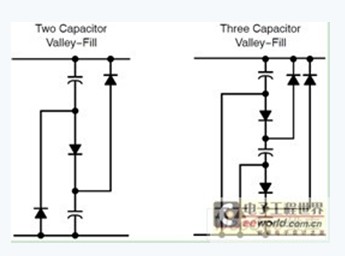
Figure 1: Typical valley filling circuit.
Although the valley-filled rectifier improves line current utilization, it does not provide a constant input to the switching regulator. The power supplied to the load will have a large ripple, which is twice the frequency of the line supply. It should be noted that four diodes are still needed to rectify the line supply, making the number of diodes used in this solution up to seven or ten. These diodes and multiple electrolytic capacitors increase solution cost, reduce reliability, and take up considerable board area.
Another option is to use an active PFC section, such as the NCP1607B, in front of the flyback converter. This approach provides an excellent power factor with typical performance above 0.98, but increases component count, reduces efficiency, and adds complexity. The most suitable power level is much higher than the power level of this application.
solution
High power factor typically requires sinusoidal line current and requires a very small phase difference between line current and voltage. The first step in modifying the design is to get a very low capacitance in front of the switching section, resulting in an input current that is closer to the sinusoidal waveform. This causes the rectified voltage to follow the line voltage, resulting in a more desirable sinusoidal input current. Thus, the input voltage of the flyback converter follows the rectified sinusoidal voltage waveform at twice the line frequency. If the input current remains at the same waveform, the power factor is high. The energy supplied to the load is the product of voltage and current, which is a sine squared waveform. Due to the energy transfer of this sinusoidal square waveform, the load will experience twice the ripple of the line frequency, essentially similar to the ripple present in the valley fill circuit.
As mentioned above, the input current must be kept in a nearly sinusoidal waveform to achieve a high power factor. The key to high power factor is to prevent the control loop from being corrected for output ripple by maintaining the feedback input at a constant level associated with the line frequency. One option is to increase the output capacitance significantly, thereby reducing the amount of 120 Hz ripple, which may be required in some applications. If the frequency is higher than the visible light perception range, LEDs for general lighting applications are more tolerant of ripple. A more compact and inexpensive solution is to filter out the feedback signal back to the PWM converter, establishing a near constant level. This level fixes the maximum current in the power switch. The current of the power switch is determined by dividing the applied transient input voltage by the primary inductance of the transformer and multiplying the length of the power switch on.
ON Semiconductor's NCP1014LEDGTGEVB* evaluation board is optimized to drive 1 to 8 high-power, high-brightness LEDs such as Cree XLAMP® XR® E/XP® E, Luxeon® Rebel, Seoul Semiconductor Z® POWER® or OSRAM Golden Dragon?. The design is based on the NCP1014, a compact fixed-frequency pulse-width modulation (PWM) converter that integrates a high-voltage power switch with internal current limiting. Since the NCP1014 operates at a fixed frequency, the current cannot rise above a certain point; this point is determined by the input voltage and the primary inductance before the end of the switching period or conduction time. Due to the on-time limit, the input current will follow the waveform of the input voltage, providing a higher power factor. The relevant circuit diagram is shown in Figure 2.
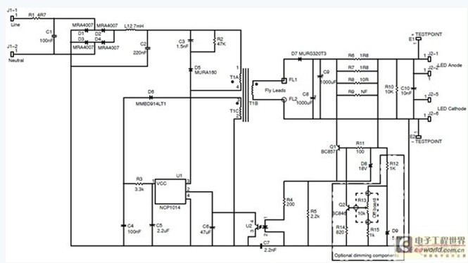
Figure 2: Circuit diagram of the NCP1014LEDGTGEVB.
designing process
Higher switching frequencies can reduce transformer size, but at the same time increase switching losses. This reference design selects the 100 kHz version of the NCP1014 as the balance point. The energy efficiency of this monolithic converter is expected to be approximately 75%, so to provide 8 W output power, an input power of 10.6 W is expected. The input operating voltage range is 90 to 265 Vac. The NCP1014 includes ON Semiconductor's Dynamic Self-Powered (DSS) circuitry, which simplifies startup by reducing component count. The thermal considerations of this integrated controller determine the maximum output power. The copper area on the board dissipates heat and cools down. When the converter is operating, the bias winding on the flyback transformer turns off the DSS, reducing the power consumption of the converter. The lower operating temperature allows more power to be supplied to the load.
The following briefly introduces the components selected in each power segment of this reference design and some related selection rationale. For a detailed design process, see ON Semiconductor's Offline LED Driver Reference Design Documentation Kit for Energy Star LED Lighting Applications at:
1) Electromagnetic interference (EMI) filter
The switching regulator consumes pulse current from the input source. The requirements for harmonic content limit the high frequency components of the power supply input current. Usually the filter consists of a capacitor and an inductor that can attenuate bad signals. The capacitor connected to the input line is turned on at an opposite phase current of 90° to the input voltage. This transfer current reduces the power factor by shifting the phase between the input voltage and the current, so it is necessary to filter the demand and maintain a high power factor. Balanced.
Depending on the nature of the electromagnetic interference and the complex nature of the filter components, capacitors C1 and C2 initially select a 100 nF capacitor. The selected differential inductor L1 is used to provide the LC filter frequency, which is approximately 1/10 of the switching frequency. The inductance values ​​used are:

The actual design chosen is a 2.7 mH inductor, which is a standard inductor value. Based on this starting point, the filter is adjusted empirically to meet the conducted interference limit. Capacitor C2 is increased to 220 nF to provide interference limiting margin. Resistor R1 limits the inrush current and provides fusible components in the event of a fault. Depending on the application environment, fuses may be required to meet safety requirements. Note that the inrush current is small with a small total primary capacitance.
2) Primary clamp
Diode D5, capacitor C3, and resistor R2 form a clamp network that controls the voltage spikes caused by the leakage inductance of the flyback transformer. The D5 should be a fast recovery device rated for the peak input voltage and the output voltage reflected to the primary of the transformer. The MURA160 fast recovery diode with a 600 V rated current of 1 A is an ideal choice for the D5. Capacitor C3 must absorb the leakage energy while the voltage is only slightly increased, and a 1.5 nF capacitor is sufficient for such low power applications. Resistor R3 must dissipate the leaked energy, but does not necessarily reduce energy efficiency. This resistor is empirically chosen to be 47 kΩ. It should be noted that the rated voltage of the resistor and capacitor C3 is 125.5 V.
3) Bias power supply
Diode D6 rectifies the power supplied by the bias winding. The MMBD914 diode with a nominal voltage of 100 V at 200 mA is a good choice for the D6. The primary bias is filtered by capacitor C4, resistor R3, and capacitor C5. The selected C5 is 2.2 ?F, C4 is 0.1 ?F, and R3 is 1.5 kΩ.
4) Output rectifier
The output rectifier must withstand peak currents well above the average output current of 630 mA. The maximum output voltage is 22 V and the peak voltage of the rectifier is 93.2 V. The selected output rectifier is a 3 A, 200 V, 35 nS MURS320 that provides low forward voltage drop and fast switching time. A 2,000 μF capacitor limits the output ripple current to 25% or peak-to-peak 144 mA.
5) Current control
A constant current output is maintained by monitoring the voltage drop across the sense resistor RSENSE in series with the output. Resistor R11 connects the sense resistor to the base-emitter junction of general purpose PNP transistor Q1. When the voltage drop across the sense resistor is approximately 0.6 V, the current flowing through R11 is biased Q1 to turn it on. Q1 determines the current flowing through the LED of optocoupler U2 and is limited by resistor R4. Optocoupler U2