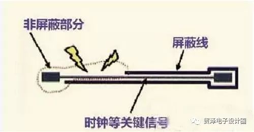
Rule 1: Shielding for High-Speed Signal Traces In high-speed PCB design, critical signal lines such as clock signals must be properly shielded. Failure to do so can lead to electromagnetic interference (EMI) leakage. It is recommended to use shielding techniques, and every 1000 mils, a ground via should be placed to ensure effective shielding and reduce EMI emissions.
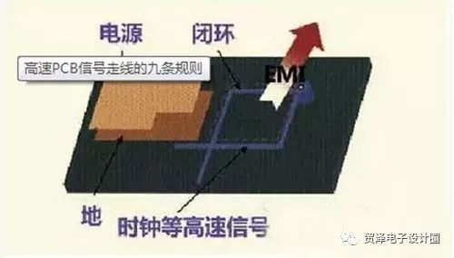
Rule 2: Closed Loop Rules for High-Speed Signals
As PCB density increases, it's common for layout engineers to make mistakes when routing high-speed signals like clocks. This can result in closed-loop structures, especially in multi-layer boards. These loops act as loop antennas, increasing the intensity of EMI radiation. To avoid this, always ensure that high-speed signal paths are designed without unintended loops.
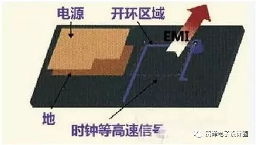
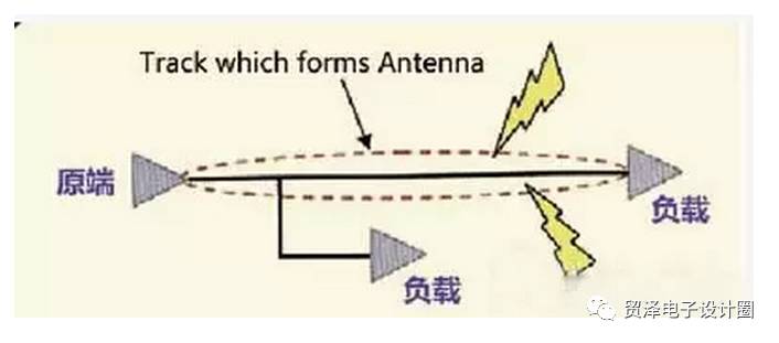
Rule 3: Open Loop Rules for High-Speed Signals
While closed loops can cause EMI, open loops are equally problematic. An open-ended high-speed signal path, such as a clock line, can act as a linear antenna, increasing EMI radiation. Always check for open loops in your high-speed signal traces and ensure they are properly terminated or routed to avoid unwanted radiation.
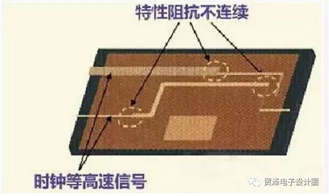
Rule 4: Consistent Characteristic Impedance for High-Speed Signals High-speed signals require consistent characteristic impedance throughout the board. When transitioning between layers, ensure that the trace width and impedance remain continuous. Any abrupt changes can cause reflections and increase EMI. Proper impedance matching is essential for signal integrity and reducing noise.
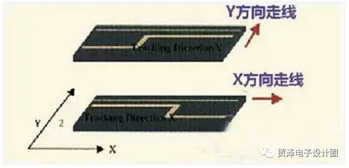
Rule 5: Routing Direction in High-Speed PCB Design The routing direction on adjacent layers should follow the vertical routing principle. This helps minimize crosstalk between signal lines and reduces EMI. By alternating horizontal and vertical routing on different layers, you can significantly improve signal integrity and reduce interference.
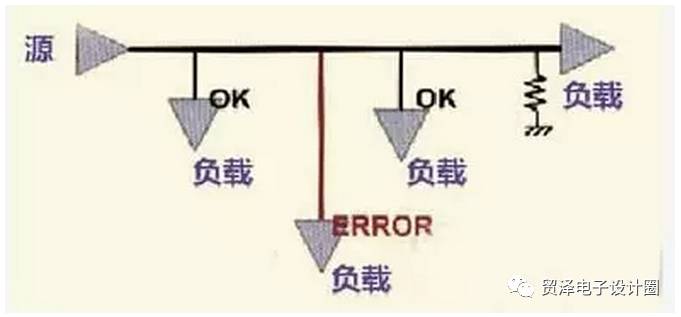
Rule 6: Topology Rules in High-Speed PCB Design Topology plays a crucial role in high-speed PCB design, especially when dealing with multiple loads. A daisy-chain topology may work for lower frequency applications, but for high-speed designs, a star-shaped or symmetrical structure is preferred. This ensures balanced signal distribution and minimizes signal distortion and EMI.
Rule 7: Trace Length Resonance Rule It's important to check if the length of a signal trace resonates with the signal frequency. If the trace length is an integer multiple of a quarter of the signal wavelength, resonance can occur, leading to increased EMI. Avoid such conditions by carefully planning trace lengths and using proper termination techniques.
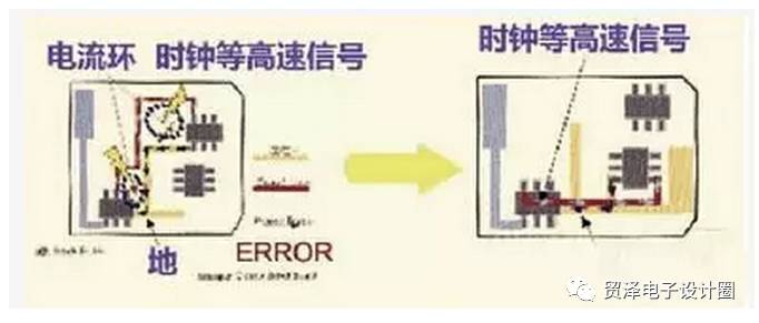
Rule 8: Return Path Rules for High-Speed Signals Every high-speed signal must have a clear and low-impedance return path. The area enclosed by the signal path and its return path directly affects the level of EMI. Minimize this area wherever possible to reduce radiation and improve signal integrity.
Rule 9: Decoupling Capacitor Placement Proper placement of decoupling capacitors is vital for power integrity. They should be placed as close as possible to the power pin of the IC. The smaller the area enclosed by the capacitor’s power and ground connections, the more effective it will be in filtering noise and reducing EMI.

From the upgrade of the existing 158.75 and 166 production lines, the process span of 182 solar panels is smaller, and the existing equipment and processes are more mature. Therefore, the difficulty and cost of new or upgraded production lines are lower, and the product yield rate is currently normal. PV industry experts suggest that the advantage of 182mm is that the industrial ecology is more mature, and it is the optimal size silicon wafer that meets the current development level of upstream and downstream, and is the first choice at this stage.
Sunket 182mm Solar Panel use 182mm 10BB/11BB Solar Cell, increases the wafer size, optimizes the layout profoundly and decreases the invalid power generation area.
1.Half Cell Technology
The half-cut cell design can decrease the power loss by the shadow effectively. The optimized circuit design not only realizes the maximum power output but also assures the reliability of solar panels.
2.MBB Technology
Sunket 182mm Solar Panel adopts multi-busbar technology. More busbars of the cell decrease the current transverse propagation path by 50%, effectively reduce the internal loss, and improve power of solar panels.
182mm Solar Panel,Mono Solar Panel,182mm Mono Solar Panel,Solar PV Module,Solar Panel
Wuxi Sunket New Energy Technology Co.,Ltd , https://www.sunketsolar.com