Today, we continue our in-depth look at the iPhone 8 Plus disassembly report, the second of three iPhones released by Apple this month. Join us as we follow iFixit to explore the internal structure of the iPhone 8 Plus.
1.

Let’s take a quick look at the main specifications of the iPhone 8 Plus:
- A new generation of A11 Bionic chip paired with the M11 motion coprocessor;
- 64GB or 256GB onboard storage;
- 5.5-inch multi-touch IPS Retina HD display with a resolution of 1920 × 1080 pixels (401 ppi);
- Dual 12-megapixel wide-angle and telephoto cameras with f/1.8 and f/2.8 apertures, optical image stabilization, 10x digital zoom, and portrait mode lighting effects;
- 7-megapixel FaceTime HD camera with f/2.2 aperture and 1080p HD video recording;
- Support for fast charging and Qi wireless charging;
- Dual-band Wi-Fi, IEEE 802.11 a/b/g/n/ac, NFC, Bluetooth 5.0, and MIMO technology.
2.
In terms of design, the glass back of the iPhone 8 series remains eye-catching. The front and rear double-glass design is reminiscent of the classic iPhone 4 and 4s models, while the overall shape is based on the iPhone 6 Plus. The biggest change brought by the glass back is the support for wireless charging. Additionally, the usual inspection marks and model numbers are now gone, but you can still find the model number A1864 on the box.
3.
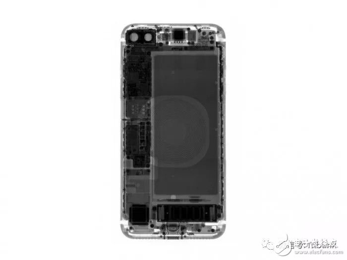
Before disassembling, an X-ray view shows the wireless charging coil clearly visible inside the device.
4.
During the screen disassembly process, iFixit noticed that the screw positions were slightly deeper than previous models, and the dents were slightly larger.
5.
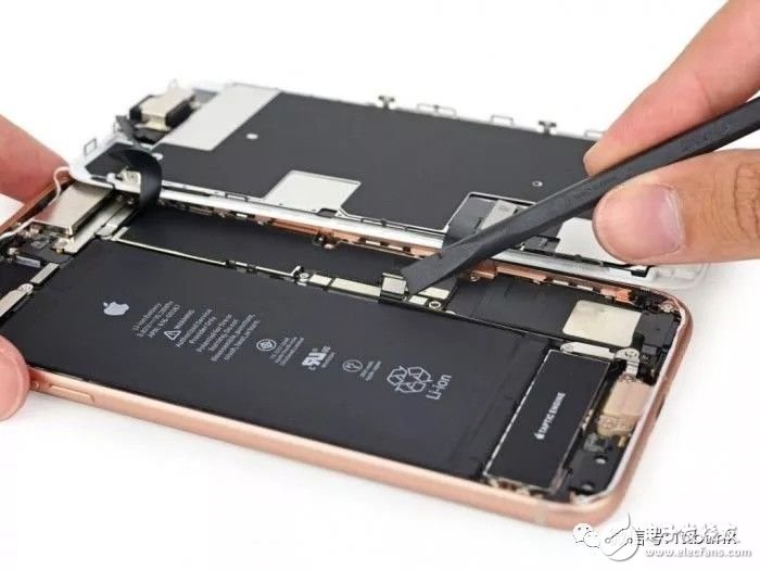
Similar to the iPhone 8, the screws securing the battery cable use the common #000 Phillips head. The tape used to secure the battery is similar to the iPhone 8, but there are two additional strips compared to the iPhone 7.
6.
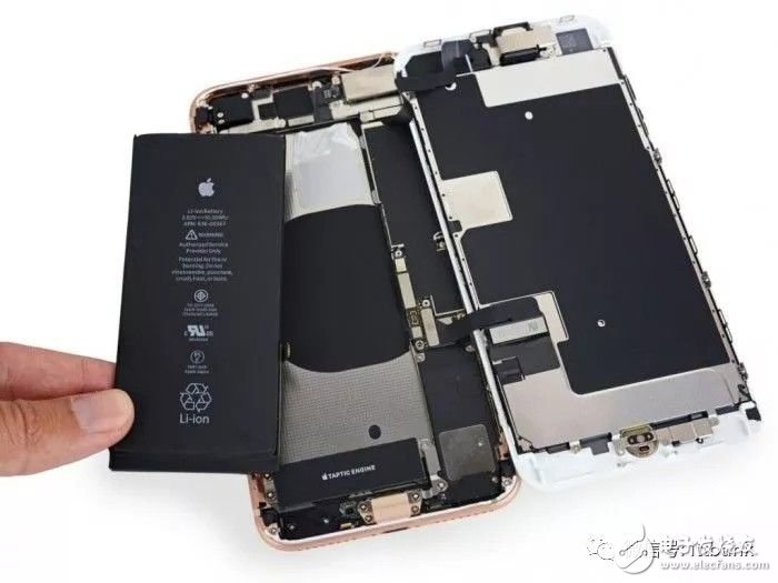
The battery has a voltage of 3.82 V, a capacity of 2691 mAh, and a power rating of 10.28 Wh. Although it's slightly smaller than the 2900 mAh found in the iPhone 7 Plus, Apple claims that the battery life is comparable or even better, especially with fast charging.
7.
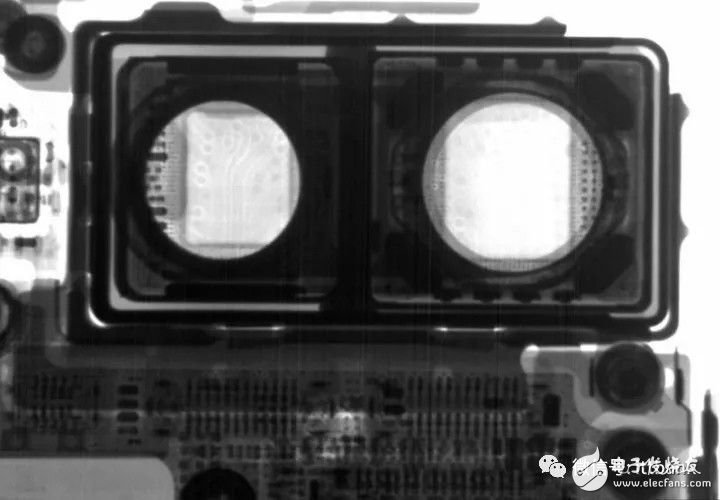
An X-ray view of the camera reveals the cable routing. After adjusting the exposure, small magnets in the corners of one of the cameras can be seen—part of the OIS optical image stabilization system.
8.
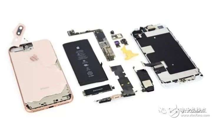
The screws securing the logic board include both standard screws and Phillips heads, as seen in earlier models.
9.
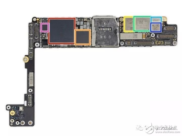
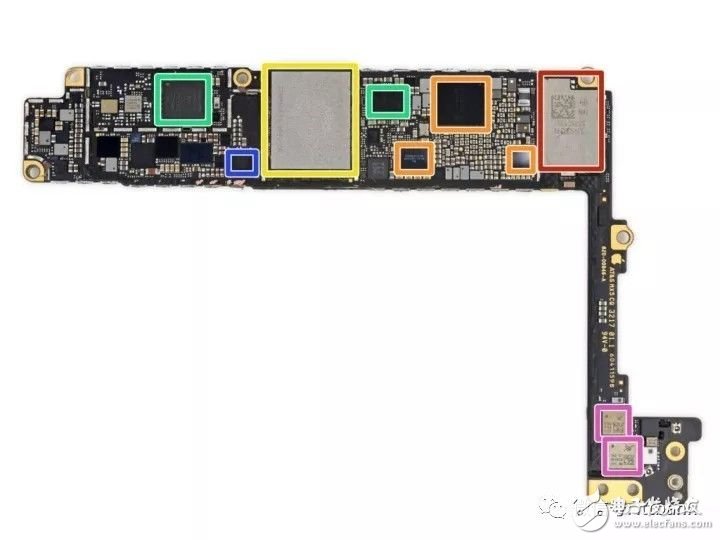
Here are the key components on the logic board:
- Red: Apple A11 Bionic CPU (Samsung 3GB LPDDR4 RAM)
- Orange: Qualcomm MDM9655 X16 LTE module
- Yellow: Skyworks SkyOne SKY78140
- Green: Avago 8072JD112
- Light blue: P215 730N71T – likely a follow-up IC module
- Blue: Skyworks 77366-17 quad-band GSM power amplifier
- Pink: NXP 80V18 NFC module
10.
On the back of the logic board:
- Red: Apple WiFi/Bluetooth/FM module
- Orange: Apple PMIC and S3830028
- Yellow: SanDisk 64GB NAND flash
- Green: Qualcomm WTR5975 Gigabit LTE RF Transceiver
- Blue: NXP 1612A1 – likely an updated Tristar IC
- Pink: Skyworks RF switches and SKY762-21
11.
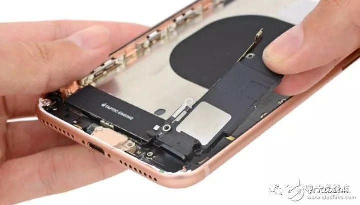
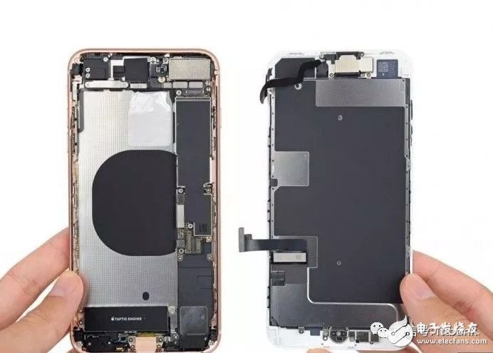
After removing the logic board, the speaker components and Taptic Engine vibration motor can be accessed, revealing details about the speaker sound hole.
12.
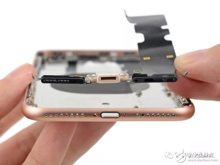
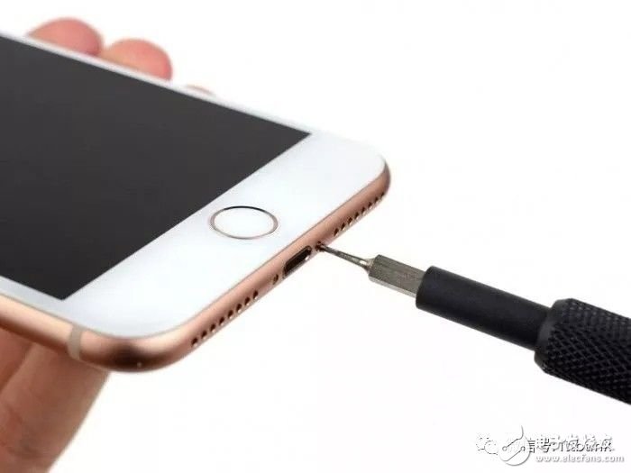
The sealing ring and Lightning interface module resemble those of the iPhone 8, with a structure designed for wireless charging and efficient heat dissipation.
13.
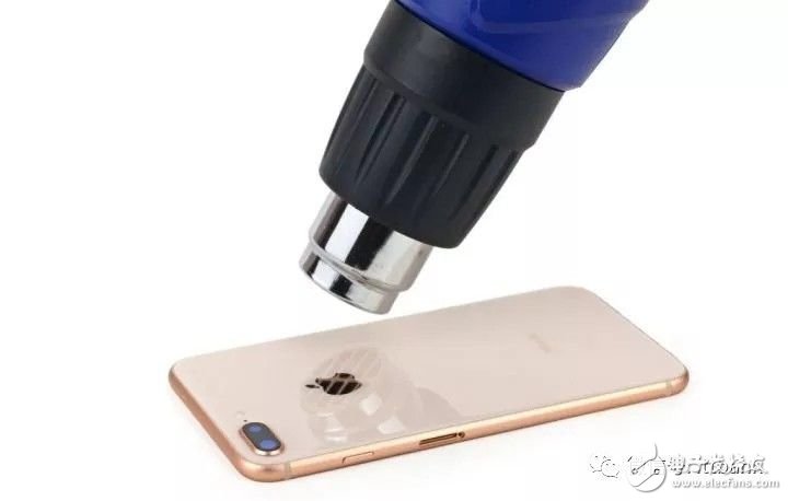
Following lessons from the iPhone 8 disassembly, iFixit tried heating the glass back, but the result was not ideal. If the glass breaks, it may require replacing the entire back frame, so using a protective case is recommended.
14.
In summary, iFixit gave the iPhone 8 Plus a repairability score of 6 out of 10.
- Screen and battery are easy to replace;
- Wireless charging helps extend the life of the Lightning port;
- Waterproof seals make repairs more complex, but improve water resistance;
- Battery connectors still use standard Phillips/JIS screws, requiring multiple tools for each disassembly;
- While Apple claims the glass is durable, once broken, it’s nearly impossible to replace just the back panel;
- Precision components and complex cables are hard to reassemble after removal.
We have got 220kV Transmission Line Substation Structure Quality Certificate from Power Industry Steel Tower Qualified Inspection & Test Center from 2001 year. Our products are made from quality sheet through bending, forming, automatic welding and hot galvanization. We can reach one-run machining length of 14m and can bend sheet of thickness up to 45mm. We adopt advanced welding procedures, automatically weld main joints and reach rank-II welding quality.
Substation Structure, Substation Steel Structure, Steel Tubular Substation Structures, Steel Structure For Substation
JIANGSU XINJINLEI STEEL INDUSTRY CO.,LTD , https://www.steel-pole.com