1 Overview
In the dedicated communication system, the conference call is an indispensable function, such as the command and dispatch of the troops, the station scheduling of the station, the three-party conference of the call transfer station, the recording of the conference, etc., and the conference function is used. At present, the conference signal synthesizer processing ASIC chips appearing on the market mainly include MC145611 of Motorla, MT8924 of Mitel, and M34116 of SGS-Thomson. M34116 has the following main technical features:
* Can be connected to 1 to 64 ways to call;
*Up to 29 groups of meetings;
* Can work simultaneously in 3 modes, conference, transparent transmission and sound generation;
* Typical bit rate is 1356/1544/2048/4096Kb/s; 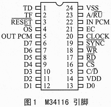
* Compatible with all PCM frame formats;
*A/μ law is optional;
*Each channel has the same priority;
* Delay from sending to receiving one frame and one time slot;
* The gain of each channel can be controlled from 0 to 15dB;
*The sound is generated from 3.9MHz to 3938Hz with a minimum interval of 3.9Hz;
* There are 7 different sound outputs on the parallel port, up to 4 different continuous frequencies;
* A sound melody that can program up to 32 different continuous frequencies;
*5V power supply;
* Compatible with TTL level inputs and TTL/CMOS level outputs.
2 Functional Description
2.1 Pin Description
The M34116 is available in a 24-pin dual in-line package with the pins shown in Figure 1.
2.2 Internal structure
When the system organizes a conference call, the output signal of any telephone interface participating in the conference must be sent to all other telephones at the same time. In other words, the signal received by the receiving end of each interface in the conference is the superposition of the analog voice signals output by all the other telephone interfaces except itself. In digital switching, due to the binary nonlinear coding (A/μ-law) characteristic of voice signals, it is not allowed to simply add signals from several binary signals. Figure 2 is a diagram showing the internal structure of the M34116. The conference chip must occupy a pair of busbars, and the PCM signal outputted by the switching network is input by the PCM I pin of the chip, and after serial-to-parallel conversion, the linearization circuit is input. The linearized each time slot (sampling) plus the attenuation or gain level of the control system port is sent to the adder, and the added result is re-linearized by POWER 10 and sent to the frame RAM. Which time slots constitute a conference is written by the control system via the data bus port. When an interface initiates a conference, the control system arranges a number from 1 to 29 for the conference. Thereafter, other noise is added to the existing conference as needed, or another conference is reorganized. The control system writes the number of each conference and the number of each time slot participating in each conference into the conference RAM by the data bus port, and the ground adder correctly combines and adds each signal. The signal output by the adder is restored to the A/μ law coded signal by the nonlinearization circuit, and finally a parallel conversion circuit is restored to the serial output and sent to the corresponding switching network PCM input bus. 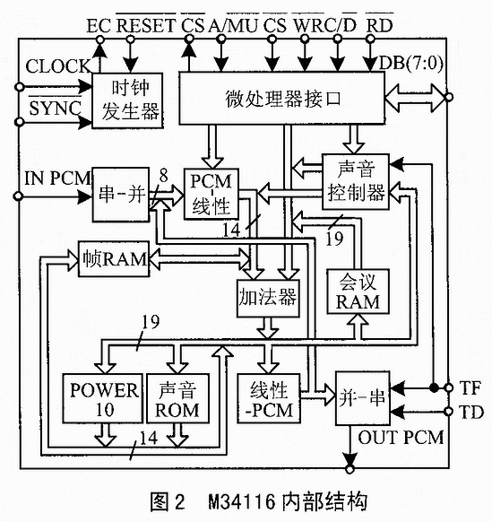
2.3 Function Description
The M34116 is designed for PCM digital switching applications and can connect to 64-party conferences and up to 29 conferences. The M34116 is connected to the switching network and the microprocessor. The switching network can use a digital switching network such as M3488 or MT8980D. After PCM encoding, the output time slot is delayed by one frame (plus one time slot) than the input time slot. Therefore, one time slot should be delayed when the conference is connected. The input and output relationships are shown in Figure 4. The M34116 has programmable attenuation or gain control for each channel of each mode of operation with an input/output range of ±15dB.
3 control word software settings
The microprocessor's control of the M34116 is achieved by setting the following command word. First, set the operation mode, send the operation mode, and perform command setting and function selection. The extension bit E=1, F1, F0 set the PCM byte format. F1, F0=00 no bit flip, F1, F0=01 even bit flip, F1, F0=10 odd bit flip, F1, F0=11 all bits flip. The M34116 must be reset to set the operating mode.
3.1 Meeting connection (command 1)
The instruction consists of 5 bytes: the first 4 bytes are data bytes. 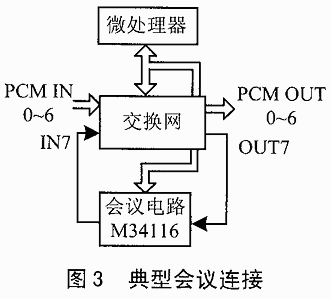 The fifth byte is the control word. The content of the first byte is the conference group number and the conference start bit S. When S=1, all the registers of the group conference are cleared to 0, and only when the first time slot of a new conference is accessed. S is 1, P4~P0 is corresponding to the conference group (1~29); the second byte is input attenuation or gain control, when AI4=1, it is gain control, when AI4=0, it is attenuation control, AI3~AI0 The value is set (0~15dB); the third byte is the output attenuation or gain control; the fourth byte is the time slot selection, and when PT=1, the PCM sampling signal is flipped before joining the conference, used for back Wave suppression; the fifth byte is the control word.
3.2 Transparent connection (command 2)
This command is another function of the M34116, which is to adjust the attenuation or gain level of the PCM input and output of one slot, delaying one frame and one time slot. This time slot is not a conference participant.
3.3 Disassembly (Instruction 3)
Demolition is a conference member, and the end of the transparent connection or the end of the generation, must be used to disconnect the line one by one.
3.4 Overflow Information (Instruction 4)
Single-byte instruction, read conference overflow, select B1 ~ B0 (0 ~ 3) by setting the gap. After this instruction, when the read is valid, the data on the data bus is read according to the selected value to determine which conference overflows.
3.5 Sound generation
Specifies the sound slot and sound sequence for gain or attenuation. The sound sequence consists of up to 4 pairs of continuous sounds and up to 32 pairs of continuous frequency melody, with a frequency range of 3.9 Hz to 3938 Hz and a continuous range of 32 ms to 8610 ms. You can specify all time slots or end with FFHEX bytes. The M34116 is constantly assigned or disconnected. The melody can be programmed as a sine wave or a square wave.
Up to 7 sounds and 1 melody time slot can be generated at the same time, and the sound and melody produce the same instruction format. The first byte is the output gain or attenuation, the second byte is the slot number, the third byte is the opcode, the FFHEX byte is the end code, and Sn7~Sn0 is the frequency interval (n ranges from 1 to 4). ), Tn is a melody (n range is 1 to 32).
3.6 Status information
The status instruction is used to read the contents of the instruction register or the sound melody register and read the status byte by specifying the slot number. These bytes include: conference number or transparent mode or sound or discontinuity, input/output attenuation or gain. In the case of the sound mode, the continuous frequency sequence of the sound is read. The first byte is the slot selection and the second byte is the control word. When the read time slot is set, the value of the subsequent read depends on the operation type (P4 to P0) of the timing. P4~P0=0, it is the disconnection state, the data read later is invalid; P4~P0=1~29, it is the conference number; P4~P0=30 sound or melody operation, the subsequent reading is the sound sequence; P4~ P0=31, which is transparent connection.
4 M34116 typical connection circuit
The typical application circuit of the M34116 is shown in Figure 5. The microprocessor is MCS-51 series single-chip microcomputer W77E58P, and the switching network adopts Mindi MT8980D. Since the switching network uses a 4.096Mb/s clock, F0i is its synchronous signal (8kHz) input. After being deasserted, the first falling edge of C4i starts the internal clock, while M34116 is started on the first falling edge of C4i. Therefore, when using the same clock, add a reverse circuit between the M34116 pin CLK and the C4i pin of the switching network. During the conference call, the control system is reliable and needs to send some prompt tones to the users attending the conference. When the external circuit inputs a square wave of frequency f at the TF end, the M34116 may output a sine wave PCM signal of frequency f at the PCM OUT terminal; when the TD is high level, the chip outputs a signal tone and simultaneously turns off the PCM voice signal. . When TD is low, the tone output is disabled and the normal PCM output is restored. The time slots from which the signal tone is output can be written by the MCU to the appropriate control word. This article only describes the implementation of the conference function, so the TD and TF pins are grounded. 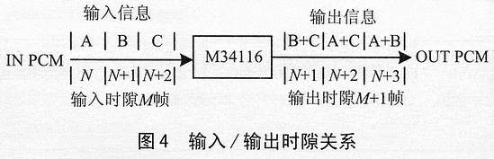
5 M34116 application instance in the private network
According to the foregoing description, through the interface circuit of FIG. 5, the processor can read and write the control word to complete the required functions. This article briefly lists the organization, joining, and disconnection of meetings. Other control words can refer to these use cases.
#define unch unsigned char
#define DATA34116 8001 //Data Address
#define CTRL34116 8000 //Control address
#define START_CONF 0XFF//The meeting starts
#define JION_CONF 0X00 //Join the meeting
5.1 Organizing meetings
/* Parameter ConfNumb: Conference number (1 to 29). MeeTInGain: Conference input gain. MeetOutGain: Conference output gain. ChannelNumb: Conference time slot. Flag: New meeting start sign*/
#pragma disable
Void ConnetConf(unch ConfNumb,unch ChannelNumb,unch MeeTInGain,unch MeetOutGain,unch Flag){
If(Flag==START_CONF){
XBYTE[DATA34116]=0x10|ConfNumb;/*Created conference number*/
XBYTE[DATA34]=MeeTInGain;/*Input gain*/
XBYTE[DATA34116]=MeetOutGain; /*Output gain*/
}
Else if(Flag=JION_CONF){
XBYTE[DATA34116]=0x1F & ConfNumb;/*Meeting number*/
XBYTE[DATA34116]=MeeTInGain;/*Input gain*/
XBYTE[DATA34116]=MeetOutGain; /*Output gain*/
}
XBYTE[DATA34116]=0x40|ChannelNumb;/*Meeting Timeslot*/
XBYTE[CTRL34116=0x07;/*write control word*/
}
5.2 Disassembly
/*Parameter ChannelNumb: Conference time slot*/
#pragma disable
Void DisconnetConf(unch ChannelNumb)
{
XBYTE[DATA34116]=0x1F & ChannelNumb;/*Meeting slots*/
XBYTE[CTRL34116]=0x0F; /*Write control word*/
}
Figure 5
5.3 Tripartite meeting
A, B, and C want to organize a meeting. Assume that the A bus is HW_A, the time slot is tsa, the B bus is HW_B, the time slot is tsb, the C bus is HW_C, the time slot is tsc, the input and output gains are all 0, and the HW_CONF is the bus of M34116.
(1) Conference initialization
ConnectConf(1,0,0,1,START_CONF);
/ / Create a meeting, the conference number is 1, the time slot is 1
ConnectConf(1,0,0,2,JOIN_CONF);//Time slot 2 joins the conference
ConnectConf(1,0,0,3,JOIN_CONF);//Time slot 3 joins the conference
(2) Time slot exchange
Connect(HWA,tsa,HW_CONF,1);//Double-link the slot of A with conference slot 1
Connect (HWB, tsb, HW_CONF, 2); / / can refer to "single chip and embedded system applications" 2002.7
Connect(HWC,tsc,HW_CONF,3);// or refer to the MT8980D data sheet
This constitutes a tripartite meeting. It is also possible to send the conference bus to HW_CONF and time slot 5 to the dedicated console to form a multi-mode or referral conference. Note that the time slot must be 5. Because the output time slot is delayed by one frame and one time slot than the input time slot.
EV Charger Tester,EV Charging Station Tester,EV Charger testing Equipment,EVSE Testing Equipment,EV Charger Test Simulator
Shenzhen Jiesai Electric Co.,Ltd , https://www.gootuenergy.com