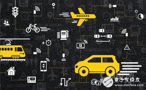
Semiconductor technology is undoubtedly an important boost to the progress of human civilization. From computers and mobile phones to mobile computing and smart devices, there is no semiconductor, and there will be no technology that has repeatedly changed the face of human life. Now, semiconductor technology is once again driving another new revolution, the Internet of Things, known as "NEXT Big Thing," continues to advance.
According to market research firm IC Insights, revenue from IoT applications will double between 2015 and 2019, reaching a market size of $124.5 billion by 2019. The number of new IoT links will reach 30.54 in 2019. Billions.
However, for the semiconductor industry, the wave of the Internet of Things is driven not only by a large number of consumer electronic components and network connections, but also by the increasing computing power of processors, data centers and mobile devices. The continuous advancement of advanced and special process technologies can achieve the required computing power, connectivity, ultra-low power consumption, multiple inductors, and system-level integration of advanced packaging. These emerging demands will drive the growth of the semiconductor market. .
IoT IC Demand Driven Process Technology
According to IC Insights, IoT IC sales will reach $19.436 billion by 2019, and the average compound growth rate for the four years from 2015 to 2019 will be 15.9%. Among them, IoT applications will accelerate the strong growth of optoelectronics, sensors, actuators and discrete semiconductor components, with sales expected to reach US$4.621 billion in 2015 and sales to US$11.647 billion in 2019. The average compound growth rate for the year reached 26%.
Secondly, the growth of the same strength is the microcontroller (MCU) and single-chip processor, the average compound growth rate in the next four years reached 22.3%. Next, the memory-related sales compound growth rate was 19.8%, the IC for specific application products was 16.4%, and the analog IC was 12.7%.
As the growth of smart phones slows down, the Internet of Things has become the next wave of driving the growth of the semiconductor market. Many internationally renowned semiconductor manufacturers have already been actively deployed. As a foundry, TSMC is determined to build an IoT ecological supply chain. The cooperation between TSMC and MediaTek is one of the results.
TSMC and MediaTek cooperate to produce MediaTek's MT2523 series products using TSMC's 55nm ultra-low power technology. This series of products is a solution designed by MediaTek for sports and fitness smart watches. It is also the world's first highly integrated GPS. Dual-mode low-power Bluetooth, a system-in-package (SiP) chip solution that supports high-resolution MIPI display screens.
In this cooperation case, TSMC offers 55nm ultra-low power consumption process (55ULP), 40nm ultra-low power consumption process (40ULP), 28nm high efficiency compact process (28HPC+), and 16nm FinFET Version process (16FF+), these processes are suitable for a variety of intelligent IoT and wearable products with energy efficiency, the main appeal is the ultra-low power emphasized by the IoT chip design.
In addition, TSMC, which has maintained its leading position in process technology, is also expected to attack new markets with a 10/7 nm process, including car networking chips such as Advanced Driver Assistance Systems (ADAS), and things that will become mainstream in the next few years. Networked application chips, etc.
Eight-inch wafers and special processes regain market opportunities
On the whole, in addition to the high-end semiconductor process technology required for some IoT chips, it is worth noting that the sensor demand brought by the Internet of Things has also re-emphasized the 8-inch fab. What are the reasons? According to the report of the International Semiconductor Equipment Materials Industry Association (SEMI), many of the large number of sensors demanded by the Internet of Things will be produced using processes larger than 90 nanometers, which has prompted many existing 8-inch factories to expand production. It is planned to have several new 8-inch fabs around the world.
SEMI estimates that global 8-inch wafer capacity will grow to 5.43 million pieces per month by 2018, returning to the equivalent of 2006, and the wafer foundry will have 43% of the world's 8-inch wafer capacity. Compared with 2006, it increased by 14 percentage points.
In addition, the low-power microcontrollers, radio frequency communications, panel drivers, touch controls, power devices, and sensors required for IoT devices do not need to be manufactured on a cutting-edge process. Some products require special process technology. Therefore, it also opens up a new world for those with special process capabilities. For example, the rise of GaAs PA is a good example.
The main function of PA is to amplify the signal. Under the demand of high-speed data transmission and low power consumption of the Internet of Things, GaAs PA with high frequency, high efficiency, low noise and low power consumption is better than CMOS PA. More suitable for the Internet of Things, and with the maturity of SiP (system-in-package), the packaging capacity of SIP PA can be further reduced, so it can be expected that with the popularity of the Internet of Things, the market size of related PA will be more expanded, which makes Businesses with GaAs process capabilities gain business opportunities.
Meets a small variety of features, mini fabs show up
In addition, the rise of the Internet of Things may also contribute to another trend that is larger and more expensive than today's semiconductor process equipment. Locking the Internet of Things for the needs of small and diverse sensors, the Ministry of Economy, Trade and Industry of Japan and 140 Japanese companies and groups jointly developed a new generation manufacturing system, which is a "minimal fab" (Minimal Fab).
The “mini fab†starts at only 500 million yen (TWD 170 million). The development goal of this mini fab is to enable automotive and home appliance manufacturers to produce their own semiconductors and sensors through a significant reduction in cost and technology barriers. The minimum floor space required for the “mini fab†is about two tennis courts, which is only one percent of a 12-inch wafer fab. The size of the machine in the production line is about the same as that of the beverage vending machine. These machines are equipped with functions such as washing, heating and exposure.
Why is the “mini fab†so low-priced and why can it be reduced in size? The main reason is to remove the need of clean room, and then use the key technology of partial dust-free, and make a special transportation system "Minimal Shuttle", using electromagnet to control the switch to prevent dust from entering. Another reason is that no reticle is used, which can significantly reduce costs. The concept of mini fabs focuses on the need for a small number of production systems in the IoT era. The wafers to be processed are about 0.5 inches in diameter, the wafers are small, and the production equipment can of course be scaled down.
It is understood that in this mini fab, the chip is cut from the wafer to a size of about 1 square centimeter. The annual output of the "mini fab" is about 500,000, and the average 12-inch fab is 200 million. At present, the "mini fab" semiconductor front-end process equipment has been roughly developed and sold. It is expected that before 2018, the back-end process equipment such as chip cutting function and package will be developed.
Different from the standardization and mass production emphasized by the computer and mobile phone market, the application of the Internet of Things is extremely divergent. This also makes the semiconductor industry have to consider the various characteristics of the Internet of Things application, and then formulate the development and marketing strategies in line with the future Internet of Things era. In order to climb the peak of another industry with the new wave.
Product Name: Car Charger
Place of Origin: Guangdong, China (Mainland)
Brand Name: OEM
Output Type: DC
Connection: Other
Rated Voltage: 12V-24V
Working Temp: 0-55℃
Weight: 36g
Materials: PC+ABS
Color: White Black
Warranty: 1 year
Suitable for:Most digital devices
SMART PROTECTION & ATTRACTIVE DESIGN ------ Intelligent circuit design protects against short circuiting,over-heating,over-current,and over-charging. Charging stops when battery is full. Car charger with blue LED indicator,which makes it convenient to find exactly where the connection should go; And the light is soft enough not to distract at night.
Dual USB Car Charger Adapter,USB Smart Port Charger ,Car Charger,USB Car Charger For Phone
Shenzhen Waweis Technology Co., Ltd. , https://www.waweis.com