The solution first uses solar energy to supply and combines the needs of people's daily life to design a multi-function solar mobile power box, and then uses MulTIsim simulation software to simulate the design of the voltage regulator module, overcharge and over-discharge protection and output port. The simulation test results are in line with the theoretical basis. The design and physical objects are built and tested, and all aspects of the output equipment can work normally. The test results show that the design scheme is reasonable and can be promoted and used.
0 Preface
The design and application of solar energy has become commonplace in the market, but based on the protection of the ecological environment in Tibet, solar energy products that combine the living conditions of local people are rare. This paper designs an environmentally-friendly and reliable solar multi-function mobile power box from the perspective of environmental protection and people's living habits in Tibet. It can be said that this design will solve the problem of people's electricity use in remote areas of Tibet.
1 concept of program design
Solar energy is a natural renewable energy source. It is rich in resources and can be used free of charge without restrictions, without transportation, and without any pollution to the environment. At present, the snowy plateau is the region with the lightest pollution and the best environmental protection in China. As an important ecological security barrier in China and even in Asia, the protection of the ecological environment is of paramount importance. The design is based on the rich solar energy resources in Tibet and the living conditions of people in Tibetan areas. It is designed with solar energy and combined with people's daily needs. It not only meets environmental protection requirements but also is easy to carry. It solves the basic daily electricity needs of the people in Tibet and can be promoted as a green environmental protection product with certain market value.
2 hardware circuit design
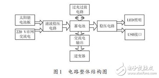
2.1 hardware block diagram structure design
The overall design hardware block diagram structure of this paper is shown in Figure 1. The power box has two sources of energy, sunlight and conventional utility. When the battery is fed, the solar energy is first charged in the case of sufficient sunlight, and the battery is secondarily charged by the 220 V power supply. The combination of two input methods is convenient and environmentally friendly. Pass the two input energies through the filter regulator circuit and then charge the battery. The overcharge and overdischarge protection circuit mainly uses the relay circuit module to detect the battery power; when overcharged, the charging main circuit is disconnected; when the battery voltage drops to a certain range, the charging circuit is turned on; when the overdischarge is detected When the electrical circuit is disconnected, the overcharge and overdischarge are prevented, and the battery protection is used. The entire circuit is powered by the battery. The system has multiple output ports, which can be used for LED lighting and charging for various digital products such as mobile phones, MP3, radio, etc. It can also output 220 V AC voltage for low-power household appliances.
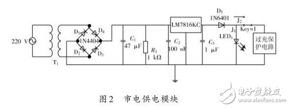
2.2 Mains power supply module
All circuits in this design are based on the application of MulTIsim simulation software.
Figure 2 shows the mains charging module circuit. When the power is turned on, the red indicator LED1 lights up, otherwise it goes out. This circuit converts the 220 V mains to 28.4 V DC through the transformer and bridge circuit, and then filters and regulates it through the RC oscillator circuit. It is then sent to the LM7815 three-terminal regulator module to output a stable DC 15 V voltage and then pass through the overshoot. The protection circuit charges the battery. The switch Key1 is a power supply mode manual selection switch. When the switch J1 is connected to select the mains charging, the red LED1 is lit. When the switch J2 is connected to select solar charging, the red LED2 is on, as shown in 1, 2.
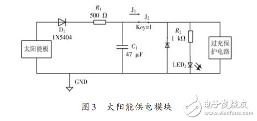
2.3 Solar power supply module
In the solar power supply module circuit shown in FIG. When Key1 is connected to J2, the solar system is selected for power supply, and the red LED 2 is lit at this time. The circuit is first rectified by the rectifier diode 1N5404, then filtered by the RC filter circuit, and finally stabilized to 15 V DC through the Zener diode 1N47744, and then the battery is charged by the overcharge protection circuit. Among them, the 1N5404 silicon rectifier diode has a maximum reverse peak voltage of 400 V and a maximum half-wave rectified current of 3 A. The Zener diode 1N4744 has a maximum power consumption of 1 mW, a stable voltage of 15 V, and a maximum current of 57 mA.
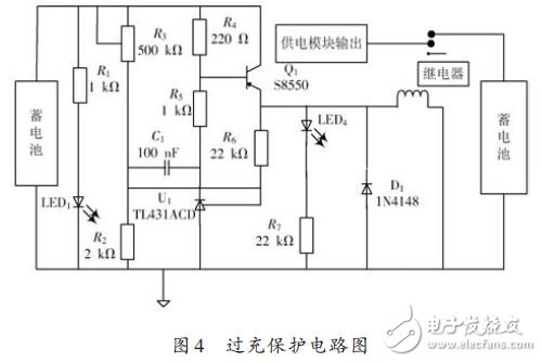
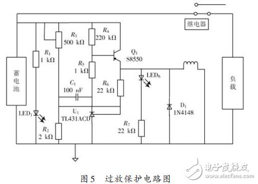
2.4 Overcharge and over discharge circuit
As shown in the figure, the overcharge and over discharge protection circuit is based on the application of the three-terminal adjustable shunt reference source TL431 and the relay to achieve charge and discharge protection for the lead battery. As shown in Figure 4, for the overcharge protection circuit, the power supply module charges the battery through the relay. When the circuit detects that the battery voltage is greater than 13 V, the green LED4 is on, the relay pulls the switch down, disconnects the charging circuit, and realizes Charge protection.
As shown in Figure 5, for the over-discharge protection circuit, when the battery voltage is greater than 12 V, the LED6 lights up, and the relay pulls down to supply energy to the load. When the battery voltage is lower than 10.5 V, the relay disconnects the discharge circuit to achieve over-discharge protection. .
2.5 output port
Figure 6 shows the design of the output port of the power box. It uses the LM78XX series three-terminal integrated voltage regulator to obtain a stable voltage output. When the LM78XX series three-terminal integrated regulator has a large output current or a long working time, the LM78XX has a large heat dissipation, and a heat sink should be added.
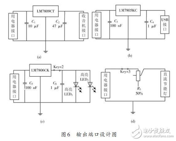
Figure 6(a) shows the output stable 9 V for radio operation. Figure 6 (b) is a USB interface circuit, the actual power box will output a number of different types of interfaces for digital product charging, such as Figure 6 (b) mobile phone USB charging part, three-terminal integrated voltage regulator LM7805 get stable DC 5 V output Since the voltage required for charging the mobile phone is (5±0.5) V, it is just suitable for charging the mobile phone. When the red LED3 is lit, it indicates that the mobile phone can be charged at this time. Figure 6 (c) and (d) are connected to the lighting load. When the switches Key2 and Key3 are turned on, by adjusting the sliding varistor R2, R3 can change the intensity of the light, thereby achieving the light intensity required by the user, and increasing the design. Humanize.
SHENZHEN YINZHIGUAN DIGITAL TECHNOLOGY CO.,LTD , http://www.yzgmusiccrown.com