1 Introduction
In traditional computer systems, serial ports (such as RS232) and parallel ports are often used to connect peripheral devices, but serial ports and parallel ports have slow communication speeds, interface monopoly is not conducive to expansion and other insurmountable shortcomings, and Universal Serial Bus (Universal Serial Bus) , that is, USB) has been widely used due to its advantages of fast transmission speed, hot plugging, convenient expansion, strong anti-interference, low cost, high data transmission quality, and saving system resources. Currently, it has become the most commonly used computer. One of the interfaces.
There are currently two main types of USB controllers: a microcontroller with a USB interface (MCU) and a pure USB interface chip. The pure USB interface chip only handles USB communication and must have an external microprocessor for protocol processing and data exchange. Typical products are Philips' PDIUSBD11 (I2C interface), PDIUSBD12 (parallel interface); NS's USBN9603/9* (parallel interface). The MCU with USB interface can be divided into two types from the application, one is the MCU designed from the bottom layer dedicated to USB control; the other is the ordinary MCU with USB interface added, such as Cypress EZ-USB (based on 8051) The biggest advantage of choosing such a USB controller is that developers are very familiar with the system structure and instruction set. The development tools are simple, but the price is relatively high, which is not conducive to product upgrades and retrofits.
However, the USB chips used in domestic products are imported, mainly provided by foreign IC design chip manufacturers such as Cypress, NEC and other internationally renowned companies. In view of the good market prospect and profit margin of USB chips, although domestic enterprises or research institutions are still only at the technical level of USB chip application development, people still hope to independently develop USB chips with independent intellectual property rights. Therefore, in recent years, many units in China have been exploring independent design of USB chips.
This paper is aimed at the USB1.1 protocol specification. Based on the self-developed USB control chip, the MCU and the USB device controller are integrated on one chip in the form of a soft core. The microcontroller uses a 14-bit instruction word length and is a single word. Section instructions and single-cycle instructions, with only 39 core instructions, are easy to master and design, and fully meet the overall design requirements.
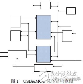
2 MCU&USB device controller working principle and overall design
The overall structure of the whole design is shown in Figure 1. The differential signal lines D+ and D- are connected to the host. When receiving, the serial data sent by the host is processed by the transceiver and USB device controller for decoding and verification, and then stored in the corresponding RAM. When sending, the corresponding data extracted from the RAM or ROM by the arbitration module is sent to the host through the USB device controller combination and the transceiver serially. The MCU primarily assists the USB controller in performing data transfer between the device and the host.
2.1 MCU design
The MCU mainly performs various interrupt processing, and assists the controller to enable the host to detect and identify the device. When the device is just plugged into the PC, the MCU initializes the dedicated function register by reading the instruction in the ROM, enabling the global interrupt GIE and the USB interrupt USBint. Enables the controller to respond to various USB interrupts in a timely manner; all interrupts are enabled when the global interrupt enable bit, GIE, is set; all interrupts are disabled when cleared. When an interrupt is serviced, the GIE bit is cleared to disable other interrupts, and the interrupt service routine is loaded, pushing the interrupt return address onto the stack. The interrupt flag bit that causes the load interrupt service routine is cleared by software before re-enabling the GIE to avoid repeated response interrupts. In the interrupt service routine, the interrupt source can be judged by detecting the interrupt flag bit. The setting of each interrupt flag bit is not affected by the GIE. During the communication between the device and the host, the MCU processes the setup packet, the in packet, the out packet, and the ack. Interrupt processing such as nak, stall packet, etc., we specify the interrupt entry addresses of USB interrupt, timer interrupt, external interrupt, GPIO interrupt are 04H, 08H, 0CH, 10H respectively; MCU also performs corresponding operations on each function register. For example, write the maximum value allowed by the input and output packets of endpoint 0, the trigger bit of the data DSQ (ie, the Data Toggle mechanism), and so on.
2.2 arbRAM, arbROM (arbitration module) design
There are two types of memory in the design: program memory (ROM) and data memory (SRAM), both of which have their own bus, which can be accessed simultaneously in one clock cycle. Both USB and MCU can access SRAM and ROM. The arbitration module is set to avoid collision when both are accessed. USB access ROM address space 100h-fffh (we store the device descriptor here), and USB access Take only the lower 8-bit data of 14 bits wide. When the USB and MCU access the ROM at the same time, the MCU takes precedence. The USB shares a general-purpose register (SRAM) with the MCU. When the USB request accesses the memory signal, the upper three bits of the address signal of the USB access memory are not equal to zero and belong to the address space of the USB access program memory. The MCU has priority when the USB and MCU access the general purpose register (SRAM) at the same time.
2.3 USB device controller design
The USB device controller is the key part of the design and is the focus of this paper. The overall module division is shown in Figure 2;

2.3.1 Transceiver design
As an analog front end of the USB interface, the USB transceiver mainly converts the analog signal sent from the host into a digital signal VP, VM to the digital phase-locked loop or converts the VP0 and VM0 digital signals sent by the protocol engine into analog signals, and completes the string. And parallel and serial conversion;
The model of the transceiver is shown in Figure 3. Dplus is a positive-phase USB differential data line and Dminu is a negative-phase USB differential data line, both of which are bidirectional. OEn is USB transmission enable. When it is low, it is a transmission function. The single-phase output port is set to high impedance. When it is high, it is used as a receiving function, and the single-phase input port is set to high impedance.

2.3.2 Dpll (Digital Phase-Locked Loop) Module
The digital phase-locked loop implements clock recovery, frequency division, and synchronous clocking; the module divides the frequency with an external 6M clock CLK, generates a 1.5M USB system clock, and locks the differential and parallel signals generated by the transceiver to avoid Produces a metastable state.
2.3.3 SIE (Serial Interface Engine) Module
SIE is the main module of the USB controller; implements protocol layer functions, packet parsing and combination, synchronization signal identification, bit stuffing and bit stripping, NRZI (non-return-to-zero inversion) encoding and decoding, synchronization fields and packet end Code detection and generation, CRC5, CRC16 check, etc.; Figure 4 is the state machine when the device receives data from the host.
![]()
It can be seen from Figure 4 that the device is in an idle state when there is no data transmission. When the low-speed device is idle, D+ and D- are in the J state. When the K state arrives, the state transition is entered. With KJKJKK as the synchronization bit, the last in the synchronization field. The 2 bits are the mark of the end of the sync field and mark the beginning of the packet identifier (PID, Packet IdenTIfier). Then enter the address state or data state according to different PIDs, followed by the address state is the endpoint state, because the address and the endpoint have 7 bits and 4 bits respectively to form a total of 11 bits, so as long as the 5-bit CRC check can be After the CRC is verified, the packet transmission is ended. The USB protocol indicates the end of the packet in two SE0 states and one J state. In the data state, it is judged whether it is the SE0 state, and the SE0 state indicates that 8 bytes of data are transmitted, because the non-SE0 state, that is, the J and K states all indicate the working state, so if there is no SE0 on the bus, the data state is always received. data.
2.3.4 ENDPCTL (Endpoint Control) Module
Two endpoints, endpoint 0 and endpoint 1, are used in the design. Endpoint 0 is a half-duplex transmission, which is used to control the transmission during the enumeration of the device. Endpoint 1 is the data transmission between the device and the host in the interrupt transmission after the enumeration is completed. Since the interrupt transmission is mainly through the input of the endpoint 1, but there is also a little output (such as the LED light output of the keyboard), in order to save resources, a small output is completed by the endpoint 0.
2.3.5 BUFCTL (Buffer Control) Module
The buffer control module is a connection bridge between the USB and the SRAM and the ROM. When the host requests the IN token state of the input data, the controller takes the data from the SRAM or the ROM and sends the data to the host or the host to output the OUT token state of the data. The received data is stored in the SRAM. It mainly controls the read/write signals according to the receiving or sending preparation signal of the serial interface engine SIE to ensure that the data can be correctly transmitted. The USB and the MCU share a general-purpose register area, usbREQUST is a request for accessing the memory signal from the USB, and usbADDR is the address signal of the USB access memory. When usbADDR[11:8] is not equal to zero, it belongs to the address space of the USB access program memory. When the USB and MCU access the data memory (SRAM) at the same time, the MCU has priority.
3 system verification environment
After completing the Verilog code design, we carried out simulation and comprehensive verification. Before using Modelsim, Synplify Pro for synthesis, and NC_Verilog for Cadence after synthesis, the speed of NC_Verilog in post-imitation is better than that of Modelsim. Efficiency; Figure 5 is an enumeration process using the NC_Verilog emulation device;

Any USB data transfer is based on successful enumeration. Only when the enumeration is done correctly, communication between the USB host and the device is being established. So enumeration is the most critical step in USB communication. During the verification process, the PC host is simulated to send various commands to the device to complete the enumeration. In pid[3:0] in Figure 5, D, 3, 9, 2, 1, and B represent Setup, DATA0, IN, Ack, Out, and DATA1, respectively. When the device is plugged into the PC, the host will continue to reset the device by SE0. At this time, the address of the device defaults to 00. Then the host sends the Setup packet for the first time to obtain the first 8 device descriptors of the device. When the device successfully returns data, The host sends the Setup packet for the second time to configure the address for the device. From the figure faddr[7:0], we can see that the address we configured for the device is 02. After that, the host obtains all 18 devices from the device through this address. The device descriptor and all the configuration descriptor sets. After the descriptors are taken, the host configures the device, and the host recognizes the device.
4 Conclusion
This paper describes the design ideas of the self-developed MCU+USB device controller. It was described in the Verilog language at the RTL level. Pre-imitation verification was performed with Modelsim, and comprehensive imitation verification was passed on Cadence's NC_Verilog. In order to further verify the correctness of the design, XILINX's Virtex xc2s2006pq208 chip and XC18V02 memory were selected in this project, and the above IP cores were integrated into the FPGA for verification. The combined results show that the protocol layer module occupies 1672 Slices (71%), 652 Slice Registers (13%), 2870 4 input LUTs (61%), and 51 bonded IOBs (36%). Using the Shanghua process, the chip has been streamed back and connected to the PC via the demo board. The PC can detect the input device for the human body, indicating that the chip fully meets the established design requirements.
Wall Mount Power Adapter mostly use as a small power source for portal electrical device . Our wall mount power range is from 3W to 48W ,All Power Adapters comply with global.
High quality ,competitive price and good servie, MLF welcome you. Please don't hesitate contact us if there is any question on the perfomance of switching power adapter .
Wall Mount Power Adapter
Wall Mount Power Adapter,Wall Adapter Power Supply,Wall-Wart Power Supply,Wall Adapter
Meile Group Limited , https://www.hkmeile.com