introduction
There are several ways to measure capacitance. But only the computational capacitance method is suitable for automatic online measurement. There are many DC charging and discharging methods and AC methods used in the application.
From the point of view of signal processing, there is no essential difference between the charge and discharge method and the communication method.
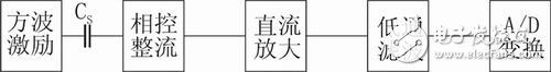
Figure 1 Signal processing flow chart of charge and discharge method
The signal processing flow of the communication method is shown in Figure 2.

Figure 2 Signal processing flow of the AC method
Therefore, the two circuits can be unified. Signal flow chart is shown in Figure 3.
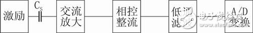
Figure 3 unified measurement conversion circuit
The phase-controlled rectifier circuit acts to shift the spectrum of the input noise signal. The low frequency noise component is moved to the high frequency band, and the high frequency noise component is moved to the low frequency band.
The phase-controlled rectified output signal is sent to the low-pass filter for processing. The high frequency components in the output noise signal will be filtered out. Therefore, the low frequency noise in the input signal of the phase-controlled rectifier circuit does not affect the final measurement result. The noise near (2n-1)fc will be moved to the low frequency, affecting the final measurement.
In order to make the measurement circuit have higher resolution, the signal input to the phase-controlled rectifier circuit should have a larger amplitude and a higher signal-to-noise ratio.
The preamplifier circuit not only amplifies the signal, but also introduces noise. The noise introduced by the amplifying circuit is determined by the amplifying circuit itself. After the signal passes through the primary processing circuit, a fixed amplitude of noise is added. Therefore, when the output signal amplitude is constant, the signal-to-noise ratio of the signal is proportional to the average value of the signal.
In the charge and discharge method, when a square wave excitation is applied, the AC amplification output is a narrow pulse, and the signal duty ratio is low. Therefore, the signal to noise ratio is also very low. Secondly, the amplified pulse signal has a large bandwidth, and the noise on both sides of the higher harmonics will also be moved to the low frequency band by the phase-controlled rectifier, which increases the low-frequency noise.
The alternating method uses a single frequency sinusoidal signal as the excitation. The signal has a large average value and thus a higher output signal to noise ratio. At the same time, since the processed signal is a single frequency sinusoidal signal, a narrowband bandpass amplifier can be used to reduce the noise introduced by the amplifier and further output the signal to noise ratio of the signal.
The AC method measurement conversion circuit can achieve higher resolution. The circuit structure is not more complicated than the charge and discharge method. Therefore, the AC excitation signal is selected to constitute the measurement system.
Excitation circuit design
The excitation circuit outputs a sine wave of a fixed frequency. The sine wave frequency, amplitude and phase are required to be constant, which is convenient for synchronizing with the phase-controlled rectification drive signal of the latter stage, and is convenient for adjusting the relative phase of the phase-controlled rectification drive signal in a wide range.
In this design, a high-precision, low-noise reference regulator is used to ensure the stability of the generated pulse signal amplitude. A high-accuracy, high-stability signal is generated using a temperature-compensated oscillator, and a high-frequency stability and low-phase jitter are obtained by dividing the frequency into a control signal. The excitation signal output is then amplified by bandpass filtering.
Voltage reference source selection
The ideal voltage reference should have zero internal resistance, and the output voltage should be kept constant regardless of whether the current flows in or out. A reference source with zero internal resistance does not exist, but an internal resistance of only one milliohm order of reference can be obtained. The working principle, parameters and selection methods of the reference source are a very important factor for system design.
Type of reference source
The reference sources are mainly Zener diodes, buried Zener diodes and bandgap voltage references. They can all be designed as two-terminal parallel circuits or three-terminal series circuits.
Zener diodes are diodes that operate in reverse bias and require a series-connected current limiting resistor. Zener diodes are generally not suitable when high precision and low power consumption are required.
The buried Zener diode integrated reference has lower noise than the bandgap type, long-term stable type, and low temperature drift. However, the output voltage is high, about 6~7V, which requires a higher supply voltage.
The bandgap reference can be as low as 1V. There are already 1.235V, 1.25V, 2.048V, 2.5V, 4.096V, 5V devices.
Voltage reference source selection
When selecting a voltage reference source, the technical specifications of the voltage reference source should be comprehensively considered for the requirements of the system. There are many technical indicators for voltage reference sources. The main indicators are: initial accuracy, output voltage temperature drift, ability to supply current and sink current, quiescent current, long-term stability, output voltage temperature hysteresis, noise, etc.
Noise is an error that cannot be compensated, so the noise of the reference source should be low.
The output voltage temperature hysteresis (THYS) is also an error that cannot be corrected. THYS is the change in output voltage due to temperature changes from hot to cold and then from cold to hot at 25 °C. Its amplitude is proportional to the magnitude of the temperature change. In many cases, the THYS error is not repeated, it is related to circuit design and packaging.
Temperature drift is usually an error that can be corrected because it is repeatable. High resolution systems require compensation. For a 5V system, if required to maintain ±1LSB over the entire commercial temperature range (0 to 70 ° C, 25 ° C as a reference point). If the reference source drift is 1ppm / ° C, ΔV = 1ppm / ° C & TImes; 5V & TImes; 45 ° C =225mV. Therefore 1ppm/°C performance is only available for 14-bit systems over the full commercial temperature range. Temperature drift performance of commonly used devices is 1ppm/°C to 100ppm/°C
Long-term stability (LTS) gives the degree of potential silicon stress or ion migration in a package or class of devices. Note that board cleanliness has a large impact on this parameter in extreme conditions of temperature and humidity. Also note that the LTS is only effective at a 25 °C reference temperature.
The ability of the voltage reference source to flow out and sink current is another important parameter. Most applications only require the reference source to supply current to the load. Many reference sources cannot sink current. Also pay attention to the load capacity of the reference source.
High Performance Voltage Reference - LTZ1000
The LTZ1000 and LTZ1000A are extremely temperature-stabilized reference voltage sources with temperature compensation. The output voltage is 7V; the temperature drift is 0.05ppm/°C; the low frequency noise is 1.2mVP-P; the long-term stability is 2mV/胟Hr.
A typical application is shown in Figure 4.
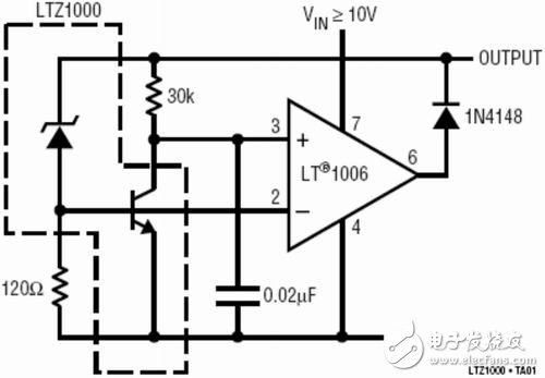
Figure 4 LTZ1000 typical application circuit
Robot Vacuum Cleaners With Mopping
Robot Vacuum Cleaners With Moppin,Robot Vacuum Cleaner With Bluetooth ,Robot Vacuum Cleaner With Gyroscope,Cleaner Robot Ultrasonic Cleaner
NingBo CaiNiao Intelligent Technology Co., LTD , https://www.intelligentnewbot.com