Ultra-wideband (wideband) low noise amplifiers are widely used in intermediate frequency and video amplifiers. This circuit is not only used to amplify video signals, but also has a wide range of pulse and RF signals ranging from DC to several megahertz or even tens of megahertz, and is widely used in signal processing. In recent years, ultra-wideband has developed rapidly in terms of secret communication and target detection. Higher bandwidth requirements claim to pass ultra-wideband signals, so the front-end pre-processing receiving circuit must be a low-noise ultra-wideband amplifier. The CMOS low noise amplifier designed in this paper is suitable for ultra-wideband systems with a working frequency range of 3 to 5 GHz. The article begins with the selection of the LNA structure, and then performs circuit analysis and design of ultra-wideband LNA structure selection.
Circuit diagramDistributed and balanced amplifier techniques are often used in traditional broadband LNA designs. In order to obtain better broadband characteristics and input matching, the two need to consume large DC power consumption. Therefore, it is not suitable for UWB systems.
At present, the application of the band-pass filter input matching structure and the parallel resistance negative feedback structure in the ultra-wideband LNA design.
The former has a large bandwidth, flat gain and good noise performance. However, a higher order bandpass filter needs to be added to the input to broaden the frequency band. The latter expands the frequency band by introducing a resistive feedback loop that reduces the input quality factor. Based on the latter, the noise cancellation technique is used to optimize the noise figure. Figure 1 shows a schematic diagram of the circuit structure used.
In Figure 1, the main amplified portion of the circuit is a parallel negative feedback Cas2code structure. C1, C2 and C3 are on-chip DC blocking capacitors, Rf is a feedback resistor, and Cf is a DC blocking capacitor on the feedback loop. Lg and L1 are input matching networks for narrowband LNAs. M1 is a common source structure, the main amplification tube, and the noise figure of the circuit and the input matching depend on the tube. M2 is a common-gate structure, and its main function is to provide greater reverse isolation and suppress the Miller effect of M1. L2, Rd, and Cd use a parallel structure to form a low Q load extended output bandwidth. M3 and M4 form a source follower to form an output stage. M1, M2, M3, and M4 together constitute a feedforward noise canceling structure. The bias circuit is omitted in Figure 1, and Vbias_1 and Vbias_2 are bias voltages.
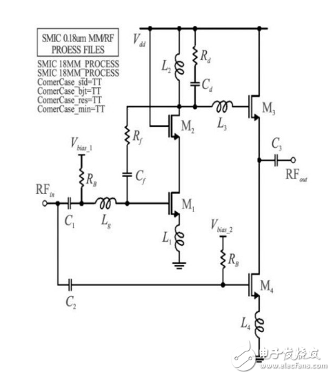
Figure 1 Schematic diagram of low noise amplifier circuit structure
Circuit Analysis and Design Broadband Input Matching AnalysisIn Figure 1, the output buffer M3 tube is removed. Since the inductively degraded structure formed by M1, M2, and L1 converts the input voltage into an output current, it can be equivalent to a transconductance stage with a transconductance of Gm. Thus, the small signal equivalent circuit of the main amplifying circuit can be obtained, as shown in FIG. 2 . The equivalent of the Gm level can be found in the literature. Here, M2 is regarded as an ideal current transmitter, and its secondary effect is ignored to obtain meaningful conclusions.
In Figure 2, Cgs1 is the gate-source capacitance of M1, Z4(s) is the input impedance of the M4 feedforward loop, and L2, Rd, and Cd form the load impedance. Gm1 is the transconductance of M1. For the impedance analysis of the ground at point X in Figure 2, we can see that:
The input impedance of the M4 feedforward loop can be expressed as:
Therefore the input impedance expression of the LNA is:
Since equation (9) is too complicated, Matlab numerical analysis is used instead of expression analysis. Under the conditions of the simulation process and feasible circuit parameters, the calculation results of FIG. 3 are obtained. It can be seen that in the range of 3 to 5 GHz, the real part of Zin is very close to 50 Ω, and its imaginary part is equal to 0 near 4.2 GHz, and the amplitude of Zin is not far from 50 Ω. This shows that the circuit has completed broadband input matching. Here, only the transistor size and the values ​​of Lg and L1 are given: M1 = M2 = 320 μm / 0.18 μm, Lg = 2.6 nH, and L1 = 0.32 nH.
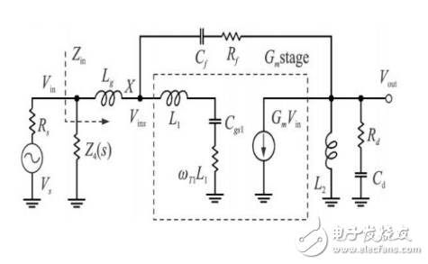
Figure 2 Core circuit small signal equivalent circuit diagram
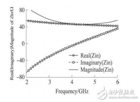
Figure 3 Zin's Matlab simulation results
Gain analysisBy analyzing and deriving Figure 2, the expression of the gain Amain(s) of the main amplifying circuit can be obtained:
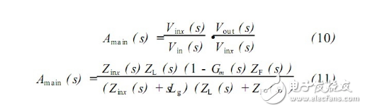
Where Zinx(s) is the impedance to ground at X. In order to increase the circuit gain, it is possible to increase the equivalent transconductance Gm and increase the load impedance ZL. However, parameters such as Gm and ZL are related to the frequency. The change of these parameters will affect the gain flatness, so the design needs to be compromised.
In order to further increase the gain of the main amplifier circuit, the inductor L3 is connected in series with the gate of the output buffer M3, and the gain boosting principle can be explained by the amplifier equivalent model shown in Fig. 4(a). CLoad can be seen as the input capacitor of M3. Figure 4(b) shows the small signal equivalent circuit of the model. The gains of analyzing small signal equivalent circuits are:
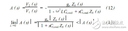
It can be seen from equations (12) and (13) that the introduction of the inductor L3 achieves the purpose of increasing the gain. When L and CLoad resonate at ω2, they have:
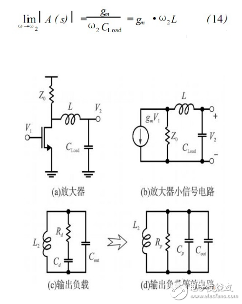
Figure 4
The output load in a wideband LNA requires a low-Q circuit.
For the 132kV Oil Immersed Power Transformer, we can produce capacity upto 180MVA. We use the best quality of raw material and advance design software to provide low noise, low losses, low partial discharge and high short-circuit impedance for power transformer.
Our power transformer are widely used in national grid, city grid, rural grid, power plant, industrial and mining enterprise, and petrochemical industry.
132Kv Transformer,132Kv Power Transformer,132Kv Power Transformer With Oltc,132Kv Transformer With Oltc
Hangzhou Qiantang River Electric Group Co., Ltd.(QRE) , https://www.qretransformer.com