Based on the bipolar junction transistor (BJT) voltage divider circuit diagram The voltage divider shown in Figure 2 has no push-pull output circuit, so much power is wasted without load. We can avoid this problem with a voltage divider based on a bipolar junction transistor. This voltage divider is especially suitable when we need high output voltage, high current, high power or when we don't need very good output voltage regulation.
As an example we will discuss a few simple applications later. These circuits have a simple adjustment of the push-pull output circuit and output voltage. They are similar to transistor type audio amplifier circuits that operate as DC amplifiers.
Figure 3 shows an example of two simple voltage dividers built around two transistors. 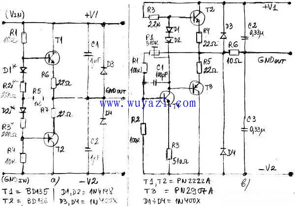
Figure 3: A simple voltage divider built with transistors.
Transistors T1 and T2 in Figure 3a are used to buffer the voltage divider output voltages constructed by resistors R1 through R4 and diodes D1 and D2. Diodes D1 and D2 function as temperature compensation, but are not required. If these two diodes are used, D1 should be in thermal contact with T1 and D2 should be in thermal contact with T2. If D1 and D2 are not used, then the R2 and R3 values ​​are increased accordingly.
Resistors R5, R6, and R7 provide simple local feedback that can be used to improve and protect the circuit. R5 is much larger than R6 and R7. The component value calculations in the circuit are similar to the component value calculations in the emitter follower circuit.
Figure 3b uses three transistors and a more efficient output voltage regulation circuit with negative feedback. The negative feedback provided by resistor R1 and trimmer potentiometer P1 stabilizes the output voltage. The output voltages +V1 and -V2 are set by P1, R1 and R2. D1 and D2 are used for temperature compensation. Resistors R4 and R5 provide local negative feedback and protect output transistors T2 and T3 to some extent.
Sometimes we need to adjust and more effectively adjust the output voltage produced by the voltage divider. In this case, we can solve these problems using a typical differential amplifier built with transistors. Figure 4 shows a voltage divider built on the basis of the five transistors T1 to T5. 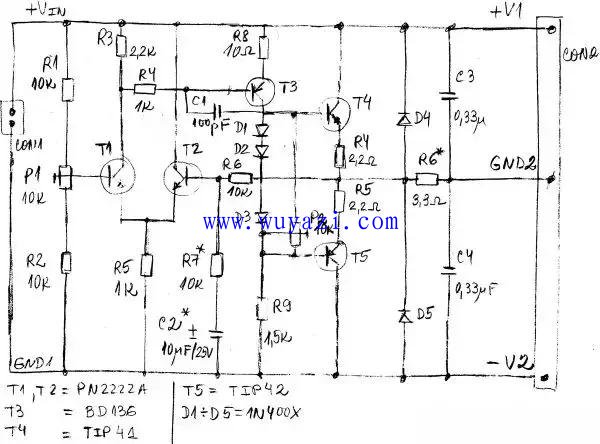
Figure 4: Voltage divider designed on the basis of a differential amplifier built into a transistor.
T1 and T2 are used as differential amplifiers. T3 is an amplifier and driver for output transistors T4 and T5. Resistor R6 provides negative feedback for stabilizing the output voltage. R7* and C2* are not required. C1 is necessary because it provides frequency compensation for the circuit.
The output voltages +V1 and -V2 are set by R1, R2 and P1. Diodes D1, D2, and D3 are used for biasing and temperature compensation of the output transistors. The trimmer potentiometer P2 is used to adjust the quiescent current of the output transistor, for example from 1mA to 10mA, depending on the load. Resistors R4 and R5 provide local negative feedback and provide a degree of protection to output transistors T4 and T5.
Environment Solution,Vacuum Toilet,Custom Pressure Flushing Toilet,Eco-Friendly Suction Car
CRRC SHANDONG CO., LTD. , https://www.crrcsd.com