Today, wireless systems are ubiquitous, and the number of wireless devices and services continues to grow. Designing a complete RF system is an interdisciplinary design challenge, where the analog RF front end is the most critical part. However, the introduction of integrated RF transceivers such as the AD9361 significantly reduces the RF challenges of such designs. These transceivers provide a digital interface to the analog RF signal chain, allowing easy integration into ASICs or FPGAs for baseband processing. The baseband processor (BBP) allows user data to be processed in the digital domain between the terminal application and the transceiver device. In addition, baseband processor designs can be easily implemented using system modeling tools such as Simulink. However, novice users may find it difficult to understand and solve this communication system problem. This paper attempts to design and implement a simple RF baseband processor for wireless transmission communication systems. The design uses the AD9361 FPGA reference design framework and is implemented on the AD-FMCOMMS2-EBZ and Xilinx® ZC706 platforms.
The first part of this article describes in detail the general design principles of the baseband processor. This section is mainly a theoretical introduction to BBP. In the second part, we discuss the actual hardware implementation of BBP using Analog Devices' AD9361 FPGA reference design. It is worth noting that the main design goal is to make the design as simple as possible and demonstrate fast wireless data transmission in a lab environment. When using and interfering with the RF spectrum, regulatory and other impacts must be taken into account.
basic designA typical RF system is shown in Figure 1, with the exception of the direct RF system. Figure 1 shows only a single data path, and the reverse direction is a mirror image of the data path. The relevant baseband processor proposed in this paper allows the data to be processed so that it is wirelessly transmitted between the two RF systems. The basic design requirements are discussed below.
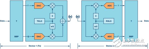
Figure 1. RF system block diagram
Repeat data on two orthogonal signals I&Q
Note that the carriers are independent and not synchronized with each other. Therefore, there is phase and frequency offset between the transmitting and receiving carriers. This will have an adverse effect on the demodulation of the receiver. An important issue is the signal reversal. The quadrature signal may reverse its effect because the offsets merge and drift regularly. A simple way to overcome this uncertainty is to repeat the same data on two orthogonal signals.
Send and receive data in serial form (bitwise)
In most cases, the RF front-end interfaces to BBP are DACs and ADCs. These are digital interfaces for analog signals. Therefore, you cannot simply send data to the DAC input and expect to get the same data at the ADC output. The data is transmitted in serial form, mapping single bit data to the full resolution of the DAC. Similarly, data is received in serial form and is demapped from the full resolution of the ADC. This provides sufficient redundancy. If these are 16-bit converters, the receiver will determine 1 or 0 from the possible 65536 data sets. With this alone, decoding can be significantly simplified.
I&Q signals are orthogonal to each other
An RF front-end device (such as the AD9361) is an I/Q transceiver. If the input is a quadrature signal, these devices are the most effective. These devices typically perform internal I/Q matching and correction along two data paths to offset any differences between the two. The rule is that the real part (I) signal is a cosine function and the imaginary part (Q) signal is a sine function.
The modulation scheme is BPSK
All common methods of deploying signal amplitude, frequency, or phase modulation can be deployed. Detecting phase differences is relatively simple. Since data is transmitted in a serial form, Binary Phase Shift Keying (BPSK) is inevitably chosen.
The bit interval is 8 samples
Data needs timing information, bit interval. The maximum possible bit interval is the sampling period. To keep the receiver simple, it takes enough time to decode the signal and make a decision. The simplest timing recovery method is zero crossing and peak detection. In this case, the peaks will be inconsistent. Therefore, zero crossing is selected for bit interval detection and tracking. There are also carrier differences between the two systems. In some cases, the sample may be ambiguous at either end of the user data. Leave 4 samples for each half of the sine signal and set the bit interval to 8 samples. Therefore, the effective transmission rate is the sampling frequency divided by 8.
Data has no direct current component
The timing and relative phase recovery is based on the zero crossing of the signal. Therefore, a single signal needs to contain no DC component. In addition, the signal is required to allow at least one zero-crossing every bit interval. The sinusoidal signal has both properties and is very much in line with the BPSK modulation scheme described above.
Data has been scrambled
The user data is arbitrary and most likely a long string of 1s or 0s. The data needs to be scrambled in order to recover the timing and phase at the receiver end to more efficiently track the signal.
Data is transmitted in packets
Because the systems are not synchronized with each other, the receiver's signal will have amplitude, frequency, and phase errors. The demodulated signal is the phase change of the transmitted signal with respect to the local carrier. The carrier may track for a period of time, select the data, and then follow it. Therefore, the design needs to be prepared for some data loss. For this reason, data is transmitted in the form of data packets. Multiple data packets can be transmitted repeatedly instead of the entire data.
Use CRC to verify packets
The data packet carries a cyclic redundancy check (CRC) code, so if there is a mismatch, the receiver is allowed to drop packets and request to send again.
Complete timing and phase correction during each preamble
The packet header carries a preamble, which is used to separate it from the received data stream. In addition, the receiver uses the timing and phase information of the preamble reset signal to demodulate the packet data.
Built-in performance indicators
The receiver also supports statistical counters, such as the number of received, discarded, or corrected packets. These counters measure and monitor performance metrics, including bit error rate and effective data rate.
In summary, data is sent and received as packets in serial form. The data packet carries the preamble and CRC. The data is BPSK modulated and demodulated on the intermediate quadrature signal before the transceiver device. Therefore, the intermediate signal frequency and the bit rate of the data are one eighth of the sampling rate. The baseband processor module and the above design details are shown in FIGS. 2 and 3 .
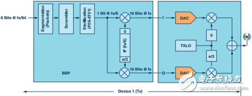
Figure 2. BBP send function block diagram
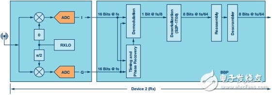
Figure 3. BBP receive function block diagram
The sender reads the data byte (character width) and converts it to a packet with a header or preamble. Add CRC to the end of the packet. Then, the packet data is scrambled and serially processed. The single bit data phase modulates the cosine (I) and sine (Q) functions before being connected to the transceiver.
In the receive direction, the off-line module recovers and tracks the relative phase of the timing interval and the modulated signal. This information is used to recover the serial data from the input ADC samples. Then assemble to the data packet and perform descrambling. At the end of the packet, the CRC is compared and if it does not match, the packet is discarded. If the CRC matches, the data is passed to the end user.
achieveThe BBP design is implemented and tested in hardware. The hardware is a combination of two evaluation boards: the Xilinx ZC706 evaluation board with Zynq FPGA devices, and the AD-FMCOMMS3-EBZ evaluation board with the AD9361 transceiver. ADI provides a complete reference design that supports this hardware. This open source design is provided free of charge in major tool versions and is fully supported and updated. See the following URL for hardware details:
ZC706
AD-FMCOMMS3-EBZ
Zynq SOC
AD9361
ADI GitHub Library
ZC706 and AD-FMCOMMS3-EBZ HDL Reference Design
AXI AD9361 IP
The ADI reference design is an embedded system that supports the Linux® framework. Contains various peripherals around the ARM® processor. The AD9361 device is connected to the axi_AD9361 IP peripheral. It transfers raw sample data between the RF device and system memory. Peripherals and devices are initialized and controlled by the Linux kernel driver. The BBP acts as another IP peripheral connected to the axi_AD9361. For historical reasons, the BBP IP is named axi_xcomm2ip. User-space applications in Linux are used to control, send and receive data between systems.
In the ADI reference design, in the transmit direction, the axi_AD9361 IP connects to the unpacking module (uTIl_upack) and in the receive direction to the packing module (uTIl_cpack). In the transmit direction, BBP data is inserted between the unpacking module and the AD9361 core. In order not to affect the default data path, BBP supports an optional data path multiplexer to select the unwrapped data source or BBP data source. BBP allows the reference design data path to be the default path and selects the BBP data source only when it is enabled. In the receive direction, BBP only connects to the AD9361 core. The reference design data path is not affected. This allows the frame to guide and set up the system unimpeded. After the system is set up, enable BBP to perform data transmission by overwriting the default data path. The BBP block diagram implemented with the ADI reference design is shown in Figure 4.
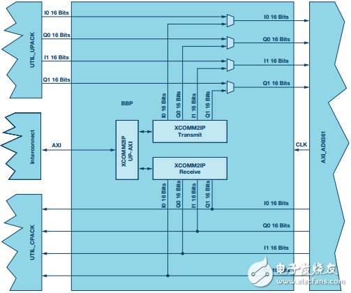
Figure 4. BBP IP block diagram
The design, initialization, and data transfer discussed in this article use a pair of this hardware. Setup requires only a pair of HDMI® monitors, a keyboard and mouse, and an antenna. The systems are completely out of sync with each other but require the same settings. In each direction, data is transmitted on different carriers. The transmit carrier frequency of device 1 is the same as the receive carrier frequency of device 2, but it is different in the other direction. However, if a single device is used in the loopback, the transmitting and receiving carriers must have the same frequency. BBP's HDL design uses the ADI library module.
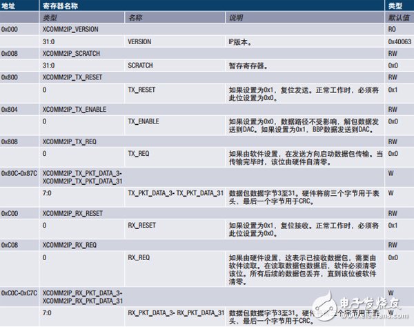
Table 1. BBP register map
Control (microprocessor) interfaceThe AXI-Lite interface is used to control and monitor the BBP through the processor. This interface module can be easily inferred using the up_axi module in the ADI common library (hdl/library/common/up_axi.v). This module converts AXI-Lite interfaces to simple memory such as read and write buses. Like any other ADI IP, add internal registers and memory. The register map is shown in Table 1.
The up_axi module port and its port mapping are described below.
Up_rstn: AXI interface reset (asynchronous low level active), connected to s_axi_aresetn.
Up_clk: AXI interface clock, connected to s_axi_aclk.
Up_axi_*: AXI interface signal, connected to the equivalent s_axi_* port.
Up_wreq, up_waddr, up_wdata, up_wack: The internal write interface. The up_wreq signal is set with address and data to indicate a write request. The request needs to be answered via the up_wack port.
As shown below, a simple register write is implemented.
Always @(negedge up_rstn or posedge up_clk)
Begin
If (up_rstn == 0) begin
Up_wack up_reg0 end else begin
Up_wack if ((up_wreq_s == 1'b1) && (up_waddr == UP_
REG0_ADDRESS)) begin
Up_reg0 end
End
End
The module performs address translation between the two. The AXI interface uses byte addresses, but the internal bus uses DWORD addresses. As a result, the up_axi module discards the two least significant bits of the AXI address to generate an internal DWORD address.
Up_rreq, up_raddr, up_rdata, up_rack: Internal read interface. The up_rreq signal is set with the address to indicate the read request. The request needs to be answered with the read data via the up_rack port.
As shown below, the same register as described above is implemented for reading.
Always @(negedge up_rstn or posedge up_clk)
Begin
If (up_rstn == 0) begin
Up_rack up_rdata end else begin
Up_rack if ((up_rreq_s == 1'b1) && (up_raddr == UP_
REG0_ADDRESS)) begin
Up_rdata end else begin
Up_rdata end
End
End
The same address translation also applies to reading. Read data is driven only when requested, otherwise it is set to zero. This is because the up_axi module passes a single read data from each address group to the OR gate. Therefore, the unselected address group needs to drive read data zero.
As listed in the register map above, BBP has three address spaces. The common register space maps to 0x000, the transmit (DAC) maps to 0x800 (0x200), and the receive (ADC) maps to 0xC00 (0x300). The software (Linux user space application) should write the transmit packet data to the buffer and read the received packet data from another buffer. The packet size is chosen to be 32 bytes with a 3-byte preamble and a 1-byte CRC.
Data interfaceFor both channels in the receive and transmit directions, the AD9361 interface core contains two pairs of 16-bit I/Q data. The core operates on the same clock as the AD9361 digital interface. In 2R2T mode, this is 4 times the sampling rate. In 1R1T mode, this is twice the sampling rate. The effective data rate is controlled by a valid signal. Therefore, in 2R2T mode, every 4 clocks are asserted once. In 1R1T mode, it is asserted once every 2 clocks. BBP is designed to support 2R2T and 1R1T modes. It uses a single send and receive channel. The internal logic operates at the sample rate in 2R2T and 1R1T modes. BBP then transmits data through the interface core at its clock frequency. This is to demonstrate clock conversion within the BBP. In many cases, the user may want to run the BBP logic at the sampling rate regardless of the interface rate of the transceiver.
Use the Xilinx primitives BUFR and BUFG to generate the sampling frequency internal clock. BUFR is a voltage divider and BUFG is a high fanout clock buffer. For this purpose, MMCM can also be used. Generate the internal clock as shown below.
Parameter XCOMM2IP_1T1R_OR_2T2R_N = 0;
Localparam XCOMM2IP_SCLK_DIVIDE =
(XCOMM2IP_1T1R_OR_2T2R_N == 1) ? "twenty four";
BUFR #(.BUFR_DIVIDE(XCOMM2IP_SCLK_DIVIDE))
I_bufr (
.CLR (1'b0),
.CE (1'b1),
.I (clk),
.O (s_clk_s));
BUFG i_bufg (
.I (s_clk_s),
.O (s_clk));
Using BUFR and BUFG ensures clock frequency locking but affects phase certainty. The maximum phase uncertainty is a single interface clock cycle. This uncertainty can be easily compensated by a four-level register array with synchronization signals. However, the design uses a dual-port RAM module for data transmission. This is also an example of an application that demonstrates common signal processing requirements. Dual-port RAM elements can be inferred using the ADI library memory module (ad_mem).
Send interfaceIn the transmit direction, the processor writes packet data to the buffer (see register map above). Then request the hardware to send the packet. BBP continuously sends packets to the device. At the beginning of the packet, check for any requests. If there are no pending requests, idle packets are sent. If there is a request to wait for processing, the packet buffer is read and sent.
The transmit logic uses a free-running bit counter that operates according to the bit width. When the bit counter is 0x0, the buffer read address is updated. Because processor requests may occur at any time during packet transmission, they are immediately captured and cleared at the beginning of packet transmission. At the start of a packet transfer, if the request waits for processing, the reply is returned to the processor interface. Use the request to choose between buffer data or idle data.
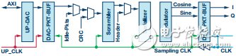
Figure 5. Send data path
The first two bytes of the packet data are set to 0xfff0. The third byte is used to indicate an idle (0xc5) or data (0xa6) packet. The CRC byte is inserted as the last byte of the packet. The CRC polynomial is x8 + x2 + x + 1. All bytes except the header are scrambled. The scrambling polynomial is the same as SONET/SDH (x7 + x6 + 1).
Cosine and sine lookup tables are used to generate modulated carriers. In 8 samples, the bit interval is equal to the complete signal period (0 to 2). Bit data is used to invert the signal. Then, the data is written to the small buffer and the interface clock is used to read from the valid signal in the AD9361 interface core.
Receiving interfaceIn the receive direction, I/Q data is monitored for header mode 0xfff0. This unique pattern only occurs once during packet transmission. Packet data can be sent so that the scrambler output repeats this pattern. The software will limit and prevent this practice. This series of in-phase data sequences of 12 consecutive bit intervals is used to reset and track the receiver timing and phase through the timing recovery block. Therefore, its timing counter is reset and its phase value is set to 0x1. The first reversal after this sequence is treated as 0x0. After this, the timing recovery module keeps its state unchanged during the entire packet transmission.
The data recovery module calculates the average value of the signal and determines the current phase of the signal. Then, it compares with the relative phase tracked by the timing recovery module. If there is a conflict, make a decision based on the signal changes in the past. This is because collisions are usually caused by phase switching.
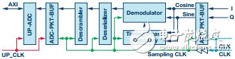
Figure 6. Receive data path
Then, the demodulated bit data is assembled into bytes and descrambled. If the transmit buffer is empty, data is written to the transmit buffer. Validate the CRC at the end of the packet. If there is a match and the transmit buffer has been written, the processor interface is notified. The software should monitor this request and, if set, clear the buffer by reading its contents. Then, the request must be cleared in order to continue the packet transmission.
The so-called mini projector is also called pico projector, TRT-Lcos Portable Projector. Mainly through the 3M LCOS RGB three-color projector and 720P film decoding technology, the traditional huge projector is refined, portable, miniaturized, entertaining and practical, making the projection technology closer to life and entertainment.
Usually the projector has certain regulations on 2 aspects:
a). Size: Usually the size is the size of a mobile phone.
b). Battery life: It is required to have at least 1-2 hours or more of battery life when it is not connected to power.
In addition, its general weight will not exceed 0.2Kg, and some do not even need fan cooling or ultra-small silent fan cooling. It can be carried with you (it can be put into your pocket), and the screen can be projected to 40-50 inches or more.
Advantage:
1. Completely replace the MP5 player, video, listening to songs, playing games, e-books, picture browsing, etc. MP5 video is affected by physical performance, the screen can not be bigger, and the screen of this thing is at least 20 inches.
2. Instead of the TV function, the machine can have a built-in CMMB function, or it can be directly connected to the set-top box to play the TV, and it can be used as a 21-inch TV during the day.
Look, it can be used as a 60-100-inch TV at night to achieve the effect of home theater; it is convenient to move and break through the traditional film and television space. Even if you are on the mountain, you can also share today's TV series, movies, and MTV with your lover.
3. Business office: instead of large projectors, it is used for company meetings; the price of large projectors is 4,000 to 14,000, and the lamp life is more than 1,000 hours, which is not convenient to carry. 30,000 hours, no need to change the bulb for 3 years, easy to carry, the salesman only needs to bring a micro projector to demonstrate the new product, which can achieve the demonstration effect.
4. Teaching: training meetings, classroom teaching; traditional projectors are not easy to carry. In school classrooms, due to the naughty students, projectors are not safe to place in the classroom and are easily damaged by students. The portability of micro projectors makes up for the teaching vacancies. In the future, teachers only need to store the materials in the projector and show them to students for teaching, saving the trouble of textbooks and handwriting with pens and chalks.
In addition, the micro-projection has no radiation, which can fully protect pregnant women and people with myopia. Its low power consumption function is 1/1,000,000 of the power consumption of color TVs. One day of electricity has completely impacted the indicators of safety, environmental protection, health, etc., and has made amazing contributions to future social development, standing at the peak of the green world as a leader.
best mini projectors under £100,mini projector pvo portable projector,mini projector portable,mini projector amazon,mini projectors for movies
Shenzhen Happybate Trading Co.,LTD , https://www.happybateprojectors.com